


In addition to voice connectivity, digital cellular wireless networks such as GSM and its enhancement, GSM-EDGE, can now provide increased data speeds up to a (theoretical) limit of 384 Kbps.
Third generation mobile networks, such as CDMA2000 and WCDMA or UMTS (Universal Mobile Telecommunications Standards) and TD-SCDMA (China only) are currently being deployed worldwide. These systems offer services such as video streaming, Internet browsing and, by using a technique called High Speed Packet Access (HSPA), they can in theory deliver downlink speeds up to 14,4 Mbps.
Development of the future infrastructure, collectively and loosely called 4G systems, is focusing on delivering higher speed and higher capacity at much lower cost. There are two technologies that are at the forefront of this development: 3GPP LTE (3rd Generation Partnership Programme, Long Term Evolution) for cellular/mobile technology, usually shortened to LTE, and WiMAX for broadband wireless access.
WiMAX has won some early backing in the access market, but several issues remain regarding roaming and switching between base stations. The major cellular network operators support LTE as the technology of choice for the future. Both 4G standards use common air interface standards based on OFDM (orthogonal frequency division modulation), and MIMO (multiple input multiple output) antenna networks. These advanced techniques allow the signal to be recovered from much higher noise thresholds, which is essential for wide area coverage.
The net effect of these complex and sometimes competing technologies is that equipment vendors need to support multiple air interface standards as well as more complex baseband processing. At the same time, these systems need to be able to provide the flexibility to accommodate planned evolution in order to deliver the increasing bandwidth that will be required in the future. They must do so at reduced cost and also, in order to meet green environmental concerns, with even lower power budgets.
In second generation systems, a macro base station was usually located at the base of the antenna with the RF power physically close to the baseband and pre-amp. One of the major system developments is in the use of distributed base stations. In these systems, the baseband processing is separated from the RF power section. Architecturally, there can be significant system cost savings in moving from a macro base station system to a distributed base station system (Figure 1).
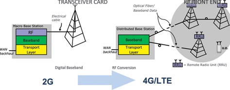
Among other requirements, a macro base station must be located within 150 m of the antenna and 50% of the RF power can be lost in the cable. Equipment upgrades and maintenance can be costly. A better solution is for distributed ‘remote radio’ networks, where the baseband is located remotely and a remote radio unit (RRU) containing the RF power amplifier can be mounted directly on the antenna mast. The RRU unit can be linked to the baseband by an optical fibre and a standard interface such as CPRI (common public radio interface) or OBSAI (open base station architecture initiative).
FPGAs in wireless infrastructure
Programmability is a characteristic that runs throughout the evolution of basestation design, since designs were often started before a specification had been completely ratified. Base stations were heavy users of ASIC devices, and FPGAs were often used as interfaces and ‘glue logic’, ie, quick fixes for design bugs or as a support function for a dedicated DSP device. As the wireless standards evolved, there was a corresponding increase in the complexity of the base station.
FPGAs were also undergoing evolutionary changes, which significantly increased their performance and logic densities. Engineers began using them for more complex functions such as digital down conversion (DDC) and digital up conversion (DUC). The flexibility afforded by FPGAs for these functions in base station design meant that FPGAs now became a key component in the design process.
FPGAs such as the LatticeECP3 family today contain many features such as multiple embedded DSP blocks, embedded memory and SERDES functions. These capabilities dovetailed with the evolving needs of wireless systems and made them the component of choice for design engineers. The flexibility of the FPGA enabled engineers to implement changes quickly, without having to wait for the next ASIC re-spin, and so time to market was accelerated.
The remote radio unit/head
The RRU function consists of a transceiver card with digital signal processing and RF conversion and an RF front end assembly comprising a power amplifier (PA), duplexer and low noise amplifier (LNA). Transceiver card designs are often broadband, with 80-90% component commonality between wireless standards and operating bands. A typical unit is shown in Figure 2.
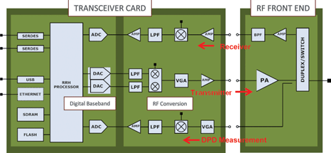
The use of an FPGA for reconfigurability allows SDR (software defined radio) techniques to support multiple wireless standards such as WCDMA, WiMAX and LTE with a common baseband. For MIMO antenna systems, the unit must provide one transmitter and receiver pair for each antenna. Next generation networks will operate at much higher frequencies than those currently deployed, usually in excess of 2 GHz. They will also need to deliver much higher data rates.
The major RRU design issue is the power consumption and cost of the RF PA. High signal peak to average power ratio (PAPR) requires the PA to transmit high power levels relatively infrequently. However infrequently this occurs, it must be allowed for in the design and this translates into higher costs. RF transistors also exhibit non-linearity at high power levels, resulting in signal distortion and out-of-band emissions.
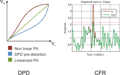
The combined effect of high PAPR and non-linearity in 4G systems can cause the PA to be operated at 20-30% of its potential output power capability and 10-15% overall efficiency; this in comparison to a GSM PA operating at 100% utilisation and up to 70% efficiency. The solution to this problem is to precondition the signal prior to the final PA in such a way that the resulting amplified RF signal is at optimal performance. There are two methods that are employed in this process; crest factor reduction (CFR) and digital pre-distortion (DPD).
Crest factor reduction works by intelligently restricting the maximum waveform amplitude presented to the input of the PA and hence the resulting peak output power. This effectively reduces the signal PAPR while maintaining the required signal accuracy and spectral characteristics. It can be used without DPD in low-power or micro base stations such as WiMAX or picocells.
DPD, on the other hand, makes the PA linear by applying a distortion to the input signal in a manner that takes into account the PA transfer characteristic, and hence nullifies any signal distortion that would be introduced as a result of the PA characteristic. It is normally used in conjunction with CFR in high-power systems with output RF power greater than 1 to 2 Watts. The effects of these techniques are shown in Figure 3.
The use of CFR and DPD techniques in RRUs can allow the system engineer to use a much lower-cost PA than would otherwise be required. Both of these techniques require a significant amount of DSP processing power to implement the necessary algorithms. Most importantly, they also require some form of adaptability, as they will need to accommodate any variations to the PA transfer characteristics that may occur over temperature and time.
The incorporation of a remote radio processor within the RRU is one solution to this problem. ASICs have traditionally been used extensively in cellular base station design; however, with their long design cycles, high fixed cost and inflexibility, they are not suited to a market that is still evolving. Discrete DSP processors would seem to be another solution for this problem, but analysis has shown that they too have limitations in multistandard base station implementations.
FPGAs, on the other hand, with embedded DSP cells, SERDES functionality and a soft processor, can accommodate all of the required functionality in a single reconfigurable chip. One such device is the ECP3 from Lattice Semiconductor. This FPGA claims to offer the industry’s lowest power consumption and price of any SERDES-capable FPGA device. The family offers multiprotocol 3,2 G SERDES with XAUI jitter compliance, DDR1/2/3 memory interfaces, powerful DSP capabilities and high density on-chip memory, all with lower power consumption and price than competitive SERDES-capable FPGAs.
While the choice of FPGA needs to be carefully considered in order to meet the physical and performance parameters of the system, it is critical that intellectual property (IP) crucial to the functionality of the RRU is available for the total system solution. As part of its IP partner programme, Lattice has teamed with Affarii, a company that has extensive experience in cellular radio systems. The combination of the LatticeECP3 FPGA with Affarii IP enables both companies to provide a flexible platform that can combine all the IP blocks necessary to build an RRU within the fabric of the FPGA.
The RRU processor is responsible for multiplexing and modulating the signal data onto the RF carriers for transmission and reception. Figure 4 shows both the Lattice IP and the IP provided by Affarii. The blocks have been colour coded to facilitate identification. The CFR configuration can be optimised for differing specific applications. The precise parameters can be determined by simulation of the maximum carrier configuration. Standard system configurations are provided in the design tools and documentation. Users can also create custom configurations for their own applications using IP models and the simulation environment supplied with the IP core.
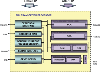
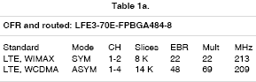
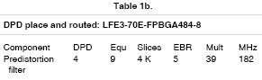
Table 1a shows the resources utilised in order to place and route the CFR IP into an LFE-70E FPGA. The configuration of the DPD operation is best determined by the characterisation of the target PA. The DPD core itself supports a diagnostic interface in order to provide analysis of the data from live or test sources. Using this tool, a detailed characterisation of the amplifier non-linearity can be performed and hence the optimum configuration can be determined for the DPD. This procedure, because it measures real-time amplifier parameters, can also highlight the need for improvements in the amplifier design. Table 1b shows the resources needed to place and route the DPD into a Lattice LFE-70EP.
The Affarii IP not only includes the CFR and DPD functions but also DUC, DDC and the adaption engine functions that are essential building blocks of a base station architecture. The major IP blocks provided by Lattice are the CPRI and OBSAI: these are high-speed interfaces that use the embedded SERDES function included in the FPGA. These interfaces link the remote baseband to the RRU. The Ethernet MAC provides for monitoring and control system functions.
Designers may also choose to use the LatticeMico32 soft processor for the RRH general purpose processing and control to save component count and cost. Advance memory interfaces and general purpose I/O (GPIO) complete the system.
For more information visit www.latticesemi.com


© Technews Publishing (Pty) Ltd | All Rights Reserved
 printer friendly version