


Ref: z2920152m
Many words have been written about the impending lead free transition, during this period of frantic discovery lots has been communicated about the reflow and alloy concerns; but the print process, which is really the first process that adds value, is often overlooked. But this is where a process can be made or broken.
Much has been documented about the differences of lead-free materials versus lead-rich materials; mainly the discussion goes along the lines of questioning the self-centring capability and the wetting characteristics. This leads onto questions such as, “What should I do with my aperture design?”, “Will I see more assembly defects?”
This article will look at these questions plus others, such as; what happens if the process window is intentionally violated?
Process window
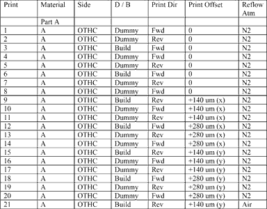
This experiment will focus on violating the print process window and measuring the response. This was achieved by including X and Y offsets to the solder paste deposits. This was realised by manually programming the automatic stencil printer with offset values, which moves the alignment of stencil to board by the prescribed amount, this value can be adjusted in 1 micron steps. To understand the influence aperture designs and offsets have on lead free assembly, we have included a stencil, which has many aperture geometries.
Stencil
A stencil was fabricated from a nickel formed blank, into this the apertures were cut with a YAG laser tool. The nickel material was chosen due to the benefits established from earlier work.
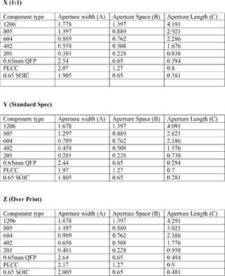
The stencil used throughout this experiment had a full range of aperture designs fabricated into the artwork, a full list of these can be seen in Table 1.
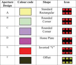
The purpose of varying the apertures within the stencil was twofold; the first was to determine if certain apertures would influence the quality aspect of SMT production, the second was to determine if aperture geometry could increase the process window in which a lead free assembly could be manufactured. All solder paste printing for the experiment was conducted using a 125 micron thick nickel/laser cut stencil. The apertures were not micro-etched or surface finished plated. A thickness of 125 microns was selected as a compromise between a 100 micron and 150 micron thick stencil. The thinner 100 micron stencil would provide better solder paste release for the smaller devices, but would inherently reduce the solder paste volume available for the larger component types. A 150 micron thick stencil was not considered because of unacceptable solder paste transfer for the smaller apertures. The metal mask was mounted in a centre-justified configuration.
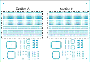
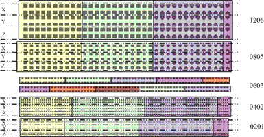
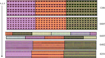
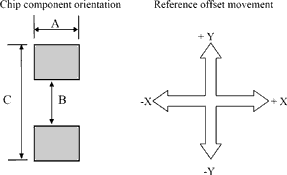
One stencil was designed for the experiment; the passive component artwork on this stencil was broken into sub designs, which provided a total of 67 designs. The breakdown of these design are shown in Figure 1a-1c and Table 1, to aid in this description the board has been split into 2 sections A and B. It can be also seen from the diagrams and table, that to help tabulate the results the aperture designs are labelled A-F and the aperture sizes have been labelled X-Z.
Board
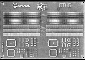
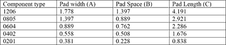
A test board was designed for the experiment; Figure 3 is a photograph of the test vehicle. The substrate was a double-sided panel that measured 140 mm wide by 204 mm long. Attachment pad metallurgy was bare copper covered by Entek plus (OSP). The ranges of passive components, which are of interest for this report, are 0201, 0402, 0603, 0805 and 1206. The Pad widths, lengths and spacing are documented in Table 3.
Note; all components were mounted in the orientation shown in Figure 2, therefore all reference to X and Y movements are as shown.
Print platform
The study was conducted using a DEK Europa platform. Before embarking on the experiment described in here, the printing machine was calibrated mechanically. Using the manufacturer’s defined procedure, the results were verified that the Cp and Cpk values passed the minimum 1,6 values. To reduce the amount of statistical 'noise' the same machine, interface and transfer heads were used throughout the experiment. The same batch of substrates throughout was also used for measurement purposes.
The following printer process parameters were used throughout the experiment
* Print speed = 80 mm/s.
* ProFlow = 300 mm cassette.
* Paste pressure = 1,8 bar.
* Print gap = 0 mm.
* Separation speed = 10 mm/s.
As part of the robustness test within this experiment, both X and Y print offsets were included, this would hopefully give an insight to the robustness of a lead-free print process. Table 5 lists the level of offsets for all the runs.
Solder paste
The solder paste sample used in this investigation is shown in Table 4. The material was suspended in a no-clean flux medium.
Reflow
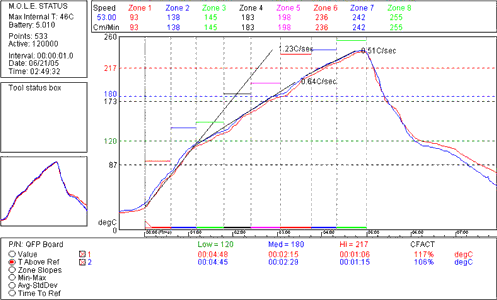
The boards were re-flowed using a standard 10-zone oven. The board was profiled to ensure a correct pre-heat, soak and peak set-up, Figure 4 shows the reflow profile used throughout the experiment, additional information about the oven set-up is shown here:
* Oven model: Vitronics-Soltec XPM2.
* Number of heating zones: eight.
* Number of cooling zones: two.
* Convection fan speed: 3500 rpm.
* Oxygen level when nitrogen active: <50 ppm.
* Conveyer speed: 53 cm/min.
* Peak temp: 240°C.
The use of nitrogen was selected for a number of runs; this schedule can be seen in Table 5
Results
Below is a recap of the factors that where included within this experiment:
* 67 individual aperture designs for each passive component.
* Offset shift in both X and Y.
* Atmosphere both air and nitrogen.
From the above list many responses were gained from this experiment and what follows shows the highlights from this.
The first set-up was focused on the effects of a standard process, during this set-up no adjustments such as offsets were included, and the reflow atmosphere was nitrogen-enriched. The results from this batch of experiments showed that with a centred print process, the assembly process was extremely robust. The next batch of results shows, the assembly yield when X and Y offset are included into the process.
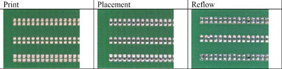
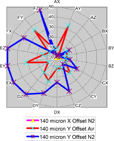
Figure 5 shows that a shift of +ve 140 microns in the X-axis with nitrogen does not cause a large number of defects (4). For clarity the photographs presented show the top left-hand corner of the 0201 chips, this includes aperture designs A at 1:1 (X), Standard Spec (Y) and over print (Z). The set of photographs shown in Figure 6 illustrate the results observed during this set-up.
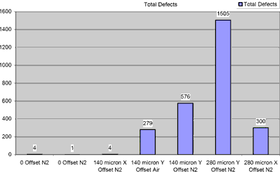
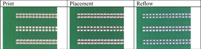
When the same +ve 140-micron offset is added to the Y-axis, 576 defects are observed. The majority of these defects were tombstones. The set of photographs shown in Figure 7 illustrate the results observed during this set-up.
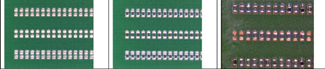
The next step in the experiment was to keep the 140-micron Y offset but switch off the nitrogen and allow the reflow process to run in air. The result from this was remarkable; the defects were noticeably reduced (279). The set of photographs shown in Figure 8 illustrate the results observed during this set-up.
The final batch of tests involved increasing the offsets to 280 microns.
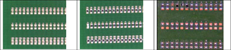
Again the response from the y-offset shift was more responsive and gave a total of 1505 defects. The set of photographs shown in Figure 9 illustrate the results observed during this set-up. A worthy observation from this set of photographs are reasonably good reflow results, which were obtained from the bottom row of 0201 components, the aperture design which corresponds to this row was AZ. The other two rows were the same shape but different aperture size; the poorer response can be seen clearly.
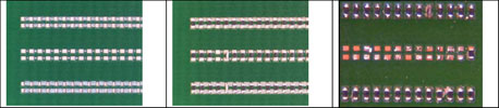
The 280-micron offset in the x-axis again was not as responsive but this test did results in 300 defects. The set of photographs shown in Figure 10 illustrate the results observed during this set-up.
As can be seen from Figure 5, if you could guarantee a print process in which the offsets do not deviate, then a fair statement would be that, 'no change' to stencil architecture is required; but this is the real world and we know that FR4 has a dimensional stability of no greater than 0,08%. Which would in the case of the test vehicle used for this experiment, potentially have an excess of 200 microns offset, therefore the tests that were conducted at 140 microns will be further analysed as these results reflect, 'real life'.
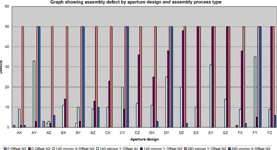
Figure 11 shows a breakdown of the defects by aperture design. For the reasons mentioned above we will only focus on the runs in which the 140-micron offsets were included. It is interesting to observe the effects of 280, but if you are running with this amount of alignment offset, the implementation of lead-free is the least of your worries.
It can also be clearly seen that from Figure 11 the addition of nitrogen (N2) has a detrimental effect on the process.
The results, which utilised air within the reflow process, show superior capability, but still certain aperture designs still show issues when 140 microns offsets are employed. Aperture design AZ shows good capability and this design is interdependent of the reflow atmosphere( AZ, a standard rectangle and overprint). This design would be the preferred design for all passive components, as it has proven that it can cope with the, 'normal' offset shifts that occur in SMT assembly.
Conclusions
During this experiment several points have been discovered: One of the most important of these is the comprehension that a centred lead-free print process should not give the process engineer any major alarm. An important aspect is to ensure that the repeatability and accuracy of the deposit is under control. As we have discovered in past investigations, the utilisation of enclosed print head technology and nickel/laser cut stencils are the enabling tools to achieve this stability of deposition.
But, of course, as we have already discussed, a utopian process does not exist within an assembly facility, therefore, the 'no problem' statement is only true if you have the luxury of manufacturing within a laboratory facility. Therefore, we need to fully appreciate the influence that stencil geometries can have on a real life lead free process.
Figure 12 shows all the combinations of aperture designs and size. A total of 67 aperture designs were used throughout the experiment. As can be seen from the results, some designs were extremely detrimental to the process, but design AZ (standard rectangle with 50 micron added per side) showed significant benefit for all passive components that exhibit standard assembly offset creep. It would seem that this slight increase of solder paste volume aids the assembly process, particularly once the solder paste placement accuracy is breached. One reason for this increased capability could be explained by the fact that the overprint not only gives a 'larger slop' area of placement, for both 'paste on pad' and 'component to pad' alignment, but the additional solder paste material balances the wetting forces during the reflow process. A further benefit to this aperture design was the fact that the O.S.P pad was tinned, which is more a cosmetic feature but, one which is ever present in the discussion of lead-free assemblies.
The addition of nitrogen clearly increased the number of defects. This could be due to increasing the wetting forces and reduced wetting time of the solder during reflow. Longer thermal reflow profiles could reduce the number of assembly defects that have been observed with nitrogen.
One strong observation from this experiment was the different response between the resistor and capacitor packages. The capacitor package accounted for approximately 80% of all the defects recorded. This defect rate was more noticeable on the 0201 and 0402 capacitor packages, once the solder paste was shifted in the y-axis. Both these packages have a high height to width ratio, which would tend to suggest that the balance of total downward forces pulling down on the component is only slightly more than the surface tension moments of the end faces; therefore when the paste is mis-aligned, the end face, which is not fully contacted with the solder paste, does not have sufficient surface tension to equal the pulling force of the opposite side. When this phenomenon happens, the chip component flips up due to imbalance of forces. On the larger chip components this is not seen, mainly because the mass of the component is greater than the end surface force.
To sum up:
* Apertures that were rectangular in profile, and include an additional 50 microns on the east and west edge, (assuming the chip component is mounted vertically) display a greater assembly yield rate.
* Using nitrogen within the reflow process, is detrimental to the assembly process window.
* Utilising the correct aperture designs can deliver a high yield rate even when 'paste to pad' or 'component to pad' offsets creep into an assembly process.
For more information contact Zalman Orlianski, Zetech, +27 (0)11 789 3230, zorlianski@zetech.co.za
| Tel: | +27 11 609 1244 |
| Email: | zetech@zetech.co.za |
| www: | www.zetech.co.za |
| Articles: | More information and articles about Zetech One |


© Technews Publishing (Pty) Ltd | All Rights Reserved
 printer friendly version