


The concerns for the environmental impact of increasing amounts of lead containing products within waste landfill sites have defined legislative and commercial pressure to implement lead-free solutions within printed wiring boards (PWBs).
Already, products for the Japanese and European markets have to comply with the lead-free requirements. Therefore, manufacturers must decide what effects this change from traditional lead solders will have on the manufacturing and test and inspection procedures that are used.
A great deal of information already exists to help those that are changing to lead-free production. The majority comes from those who have already been through the process (sic). Further information on the European lead-free roadmap, together with other useful data based on experience of manufacturers moving to lead-free can be found in the websites mentioned in references 1 and 2.
Tin/lead (SnPb) solder has benefited from many decades of experience to define the process-window, and the inspection and testing regimes applied, to ensure quality manufacture. Lead-free materials have higher process-temperature requirements and are visually different in appearance to SnPb materials. For example, the joints no longer looking shiny when using SAC alloys. Therefore, the need for more, and improved, inspection becomes ever more important for process development and on-going QC evaluation as the change to lead-free takes place. In particular, it is important to be able to assess the level of voiding within the lead-free joints and how this level may vary depending on factors such as the type and formulation of the solder paste, the reflow profile, the board finish and the board substrate. Not only is this inspection required to confirm the right process and materials for production are in place, but it will also be needed as part of on-going process control.
Digital X-ray inspection
With such a change in the materials and methods used for PWB assembly, the use of X-ray inspection has increased dramatically. This is because of X-ray's ability to inspect samples non-destructively, during production and ahead of repair and rework. X-ray is particularly useful on devices with optically hidden joints, such as BGAs, flip chips and CSPs. In addition, it is also because of X-ray inspection's ability to look within all joints of the board to confirm and quantify voiding levels, ahead of making any process adjustment for optimum PWB manufacture.
Any initial concerns that existing users of X-ray inspection systems may have about using their current equipment for lead-free applications are unfounded. Reference 3 shows that system settings may only have to be modestly adjusted, if at all, to observe the potential faults within lead-free materials, even though the removal of the lead reduces the density of the solder material.
X-ray inspection usage has also increased because of the continuing improvement in X-ray system capabilities. This has been, in part, so that analysis on the ever shrinking devices and joint sizes (eg, sub-100 micron flip chip bumps, 0201 and even 01005 components) remains possible. Firstly, this was achieved by replacing closed X-ray tubes with open, demountable, X-ray tubes within the X-ray systems permitted enhanced magnification and system resolution[4]. Secondly, X-ray systems are now able to tilt the detector, instead of the board, to achieve the oblique angle views that are so necessary to allow proper investigation of the joint interfaces. By tilting the detector, the oblique views are all available without compromising the achievable magnification, so necessary for the shrinking device sizes[5]. If a 2D X-ray system cannot offer oblique angle views, then the bulk of the solder joint itself (such as a BGA solder ball) may prevent adequate analysis of the joint quality. Finally, the most recent advance has seen X-ray systems become available that offer digital detectors instead of analogue versions. Such digital detectors can provide realtime X-ray inspection at up to 16-bit greyscale sensitivity within the captured image[6]. This improvement in sensitivity represents an increase of up to four times that of the earlier, analog detectors, and is provided at higher resolution. This much greater greyscale sensitivity allows far better visual separation of similarly dense features within applications, such as non-conductive die-attach, voids in packages, voids in moulding compounds and glob-tops, microvia inspection, etc. Without this enhanced sensitivity, analysis of such applications would prove almost impossible.
Voiding and joint interfaces
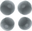
An example of where digital X-ray imaging provides a capability for process control that was not possible with analogue X-ray detectors can be seen in Figure 1. Here, a single BGA ball is seen at an oblique angle view.

The sensitivity within the system and detector makes it possible to see the shape of the actual joint interfaces, due to the flattening of the solder spheres at the contact surfaces. This creates contrast-resolvable ellipses within the collapsible BGA solder ball. Figure 1 also depicts a large void within the ball. The location of the void adjacent to one of the interface ellipses can be clearly seen in Figure 2, where the same BGA ball has been imaged at different oblique views. The presence, or absence, of these ellipses can help to indicate the joint quality, as an absent 'ellipse', compared to neighbouring solder balls within the device, would strongly suggest an open joint.
The presence and quantity of the voids within the joints of a PWB, in all components and not just in area array packages, can be a very sensitive indicator of the overall process quality. This can be easily monitored by the X-ray inspection system. Therefore, continuous monitoring would show if the level of voiding had become too high, or identify an increasing upward trend, which would provide good feedback to confirm the process quality. Of course, the presence of voiding may also be indicative of other potential problems within the PWB, such as moisture ingress to devices, manufacturing problems in devices and surface finish effects from the bare board.
This last problem has been seen only most recently using digital X-ray systems and shows many small voids located within the ball to pad interface. As there are so many voids it has been called 'champagne voiding' by some. An example of how this defect looks within an X-ray image is shown in Figure 3. The champagne voids are all in the interfacial region, instead of in the bulk of the solder ball, the traditional location of process induced voids. The possible cause of 'champagne voiding' is still being widely discussed, as it appears on different board finishes with both lead-free and tin-lead solders. Reference 7 contains some further information on this failure mode that, whatever the cause, results in joint failure after accelerated life testing. Without the use of digital X-ray imaging and its superior greyscale sensitivity, the small density variation of these tiny voids when X-raying through the whole of the much more dense solder ball would be difficult, if not impossible to resolve.
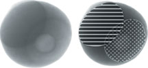
The presence of voiding should not necessarily always be considered as a process failure, however. The IPC 610-C document indicates that less than 15% voiding within a BGA ball is a pass and even up to 25% voiding does not constitute a failure, but should indicate a process review. To put this level of voiding into perspective, Diagram 1 indicates the relative size that a single void would need to be to give a 15% void percentage under X-ray inspection.
Finally, there appears to be some discussion within the industry suggesting that having a small quantity of voiding, albeit of the right quantity, size and location, may allow stress relaxation of the joint to occur. Such voiding is thought to reduce the susceptibility of the joint to thermo-mechanical fatigue mechanisms and improve long-term reliability. It is outside the scope of this paper to comment any further on this view.
The sensitivity that digital X-ray inspection provides when combined with oblique angle views, therefore, is not just in the presence and quantity of any voiding, but also in its location(s). The difference in location may help to identify the cause of 'excessive' voiding; ie, whether it is process, device or board related - or a combination thereof.
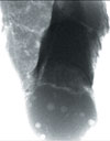
As digital X-ray inspection offers this enhanced capability across all device joints, it is, therefore, not just limited to BGA and other area array device applications. For example, it can also be used for downstream failure analysis, such as that shown in Figure 4. In Figure 4, a lead-free LCCC has been thermally cycled many times, which has caused fatigue cracking. Without the additonal sensitivity within the digital systems, such results could be missed.
Choosing lead-free solder
A recent set of experiments by Soldertec/Tin Technology investigated three different lead-free solder pastes placed on three different board substrates to ascertain the best combination for a particular application. The three lead-free solders were all tin/silver/copper alloys from different manufacturers. The three PWB materials were FR4 and two different types of CEM3. All of the boards, with whichever combination of solder and board, were soldered using the same reflow profile and had the same board finish. The initial results from testing the finished boards for mechanical strength, standard quality control measures, solder fillet shape and joint inter-metallic compound layer thickness were virtually identical for all the samples
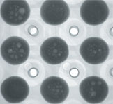
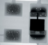
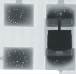
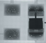
The only variation that was seen in the boards, post-production, was the level of voiding when seen under the digital detector of the Dage XiDAT XD6600 X-ray inspection system. Intuitively, it would be assumed that having two different board materials would be the cause of any variation in the voiding levels. However, the results of Figures 5, 6 and 7 show the FR4 boards (designated C) and one of the CEM3 board types (designated A) behaved in a similar fashion as each other in terms of voiding. However, the second CEM3 board material (designated B), irrespective of solder alloy used, continually had less voiding than the other two board types. In images 5, 6 and 7 only one type of solder paste (designated 3) is shown for brevity, but the results were consistent across the other two solder pastes. Overall, these images show that the look of solder joints using lead-free materials can be very different from what would have been expected, even when similar board materials are used. As such, it reinforces the need to implement an adequate test and inspection regime so as to confirm and monitor the voiding levels to ensure an optimised production process.
Conclusion
The improvements made to the capabilities of X-ray inspection systems over recent years, offers the opportunity for better and subtler inspection of PWB joints. In particular, the enhanced sensitivity of digital X-ray systems now provides an opportunity for a clearer investigation, and continuous monitoring, of the level of voiding within all PWB joints.
As a result, there is now firm evidence of at least two types of voiding that can occur within BGA balls. The first void type being the established 'process control', are voids of air bubbles trapped within the bulk of the solder ball, formed during the SMT process. The second void type being so called 'champagne voids', where many small air bubbles are located at the ball to pad interface. The morphology and location of these two different void types can be clearly defined and differentiated within the images produced by the digital X-ray system because of its enhanced greyscale sensitivity.
Finally, when implementing the change to using lead-free solders, digital X-ray systems offer a non-destructive way of assessing joint quality during qualification programmes. This will allow an evaluation of the appropriate board/solder combination to be made for each application, as well as help to maintain process reliability once a selection has been made.
References
[1] www.lead-free.org, www.smartgroup.org and www.leadfreesoldering.com.
[2] Wickham M., Brewin A., Zou L. and Hunt C.P., "Report MATC (A) 141: Code of Practice for the Use of Electronic Components and PCBs in Lead-Free Processing" UK National Physical Laboratory.
[3] Bernard D., "Implications of Using Lead-Free Solders on X-ray Inspection of Flip Chips and BGAs", Proceedings of SMTA International, Chicago, September 2003.
[4] Bernard D., "X-ray tube selection criteria for BGA/CSP X-ray inspection", Proceedings of SMTA International, Chicago, September 2002.
[5] Bernard D., "Selection Criteria for X-ray Inspection Systems for BGA and CSP Solder Joint Analysis", Proceedings of Nepcon Shanghai, 2003.
[6] Bernard, D. and Ainsworth, S., "Comparing Digital and Analogue X-ray Inspection for BGA, Flip Chip and CSP Analysis, proceedings of APEX, Anaheim, CA, 2004.
[7] Bernard, D. and Bryant K., "Does PCB pad finish affect voiding levels in lead-free assembly", Proceedings of SMTA International, Chicago, 2004.


© Technews Publishing (Pty) Ltd | All Rights Reserved
 printer friendly version