


Wave soldering with lead-free materials is probably the most demanding of the changes to traditional assembly methods due to the higher temperatures associated with the solder. Design plays a key role in zero defect and more reliable products, its important to take a fresh look at design rules and use every trick in the book.
In air there is likely to be an increase in dross production and with the higher tin content, the cost of running the machine will be higher. To date, most of the research experience in wave soldering with lead-free materials has been using nitrogen inerting. Most of this author's trials and much of the Japanese industry has been in air.
A full report on the soldering trials should be produced highlighting any soldering problems encountered. This should be attached to any new design assessment form which should accompany all new prototype production designs. If specific soldering faults are encountered, or the correct jigs or support clips are not provided, the soldering section of any design review should not be approved. A design review and checklist for wave soldering process introduction is available from the author as a process checklist.
Some of the key items are listed below:
Fluxing
* Periodic measurement of flux g/m squared.
* Flux penetration in plated through holes minimum once per day.
Preheat
* Bottom side board temperature prior to wave contact.
* Top side board temperature prior to wave contact.
* Temperature profile with real production board.
* Preheat atmosphere in nitrogen
Wave solder
* Solder wave contact time per wave.
* Quantity of solder bar added to the solder pot: tin/silver/copper kg; tin/silver kg; tin, tin/nickel and tin/silver bars for top-up.
One solder sample taken per week, dated and held for assessment. Sample must be taken from the running wave. One sample taken prior to production starting.
Solder dross
* Quantity of dross remover per day kg.
* Sample of dross retained per week and dated.
* Payment or allowance provided per kg from supplier for dross.
Printed boards
* Number of PCBs soldered per day and type.
* Hold one blank board per batch and dated for future reference.
* Sample of breakout strips retained and dated per week with machine settings.
* (Possible measurement of exposed copper dissolution and compared with temperature and contact time setings).
* Any sample boards held should be dated and all process information held for future assessment.
Inspection
* Record of the number of defects found and reworked.
* Record the location of defects reworked.
* Photograph different defect types, locations and date.
* X-ray inspection of single-sided boards for solder rise in the hole to maintain reliabiity.
Since recent trials have shown there to be an increase of solder shorts when soldering in air, further process changes will be necessary to optimise the process or improvements in general board design. The use of solder thieves on surface mount packages is a necessity, as are drainage pads for high pin count or closely spaced connectors below 0,1 mm. The use of solder thieves and drainage pads are known to enhance any circuit design and improve the yield. Although there has not been any visible increase in the incidence of solder skips during surface mount or wave soldering, there has been some increase in solder-balling. Solder balls adhere to the solder-resist coatings, selection of the best coating and the impact on the visual results in a no-clean process is very important to many users.
It is inevitable that with the increase in soldering temperatures with lead-free materials there will be the potential for board sag during pre-heating or wave contact. Consequently, design engineers should consider the use of centre board support areas on the base of the board. The support of the board during processing can improve the soldering yield on existing processes and provide a more stable process with lead-free solders. It is also less likely to cause component movement and lead lift on topside reflowed parts if temperature increase to just below reflow.
Recently the erosion of copper tracking has been highlighted as a potential issue. Recent testing has not shown this to be a issue with temperatures between 260-265°C. Temperatures above this in the range of 270-280°C have shown to be a potential issue. In recent months solder bath erosion has been highlighted as a problem. Stainless steel used for parts of the solder wave have been attacked by the high tin content tin alloys. The real reason why this occurs is still not clear but suppliers are investigating the use of different stainless steels and coating the parts of the wave affected.
The following procedure may be used when setting up a wave soldering system for a new board design, or when evaluating the changes necessary for lead-free soldering. (A CD-ROM 'Wave Soldering Lead-Free Process Defect Guide' covers much of the steps outlined in this article and available at www.leadfreesoldering.com) Only fully populated boards should be used. The component lead length should be checked along with the correct position of all surface mount components. The samples boards should be soldered with all the necessary jigs, support wires or clips in place to prevent any sagging of the boards, which changes the drainage characteristics of the solder wave.
The Engineering Department should specify the flux to be used for the new design or lead-free trials. It is probable that when adopting a lead-free process, consideration may be given to a more environmentally-friendly fluxing material eg a water-based VOC-free flux. The speed of the conveyor should initially be set at approximately 3,0/3,5 ft/min for double-sided and multilayer boards and 4,0 ft/min for single-sided boards. The solder temperature should be 260-265°C when using Sn-alloys.

Fluxing operation
The spray fluxer should be set-up and checked for correct operation using a sample unsoldered board, which should be removed just after passing through the fluxer and the air knife. There should be evidence of a thin coating of flux over the complete board with evidence that the flux has just entered the plated-through-holes.
In the case of foam fluxers, the flux head should be stable and generate the smallest bubbles possible when adjustments have been made to the air pressure. Using an unsoldered board, or a glass Lev Check, confirm that good contact is being made with the foam head. Since when using the Lev Check, the foam head is depressed, it is sensible to check that the foam bubbles making contact are relatively small.
In the case of both fluxers, the air knife should be set to remove excess flux from the base of the board. In the case of spray fluxing with plated-through-hole boards the air knife should be adjusted vertically to help flux rise into the plated-through-holes.
To monitor flux penetration into through-holes using a spray unit, a piece of thermal fax paper can be placed on the top side of the unpopulated PCB and passed through the spray fluxing system. There should be evidence of the flux wetting the paper due to the flux penetration. Using the air knife at 90° to the board will help flux rise and allow the amount of flux applied to be reduced. It is common to encounter poor solder rise on any board regardless of the surface. Although it is easy to overcoat the board with flux and get good results, the trick is to get the good results with a minimal deposit. With the possible slower wetting of lead-free solders, the correct application of flux must be monitored otherwise poor results may be incorrectly attributed to the use of the new solder.
Pre-heat operation
A fully populated assembly should be passed through the machine to establish the temperature profile. This should be carried out with the fluxer and solder wave switched off. The assembly may have been previously soldered to locate the components in position. The temperature on the topside of the board should reach a minimum of 120°C prior to passing over the solder bath.
Either temperature labels, or the Mole profiler, can be used for this operation. The profiler is preferable since it provides a full record of the profile for future reference. If the profiler is used, thermocouples should be positioned both on the bottom and on the topside of the board. The probes should be soldered in position using high temperature solder and only the leads held in place with tape. The additional probes should be located either in areas of the board where there is the greatest heat sinking effect, or to make sure that temperature sensitive components are not damaged by the increased temperatures.
In the case of surface mount boards, the termination points of selected parts on the underside of the boards should be checked. There should be no more than an 80°C temperature difference between termination temperature and solder wave temperature prior to hitting the first wave. The difference between the topside and the bottom of the board will depend on the type and density of the board.
If topside surface mount components are included in the design, the peak temperature over the wave is also important. Fine pitch terminations reflowed again during wave contact can be lifted leading to open joints. This can occur due to the increased movement of the board during wave contact, since all boards do flex during such wave contact.
A record of the profile file name saved on the computer should be recorded for future reference along with a copy of the profile attached to the test result report. The file reference should be the board name or board reference number for ease of location.
A test board should be passed through the machine with the fluxer and pre-heater section operating, and the board should be removed prior to passing over the solder wave. There should be no evidence of solvent left on the underside of the board which may cause gassing and spitting during wave contact. The visual appearance of flux on the base of the board after preheating will vary depending on the flux type and the solids content. When successful soldering results have been obtained, a visual check like this will provide a mental picture of the resulting process. If the soldering performance changes, it allows each stage in the process to be rechecked for changes.
Solder wave operation
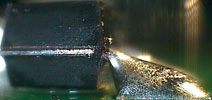
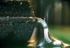
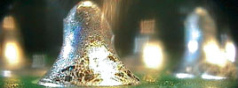
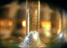
As the board goes through the solder wave it should not sag. If it does, the support is inadequate and should be reviewed particularly in the light of lead-free soldering. Unfortunately if a design change is necessary to provide adequate support it will be difficult (if not impossible) to carry out at this stage. If surface mount components are positioned on the bottom of the board then the double wave should be used. The solder contact should be checked by using the Lev Check before processing the prototype boards. It can be valuable to check (through the glass plate) for flux gassing, which can affect satisfactory soldering of chip components. It also allows the drainage of solder to be investigated with components glued to the base of the plate. In the case of lead-free soldering in air, the drainage is different from that experienced with existing tin/lead solders.
The contact width on the solder wave should be approximately 15 mm for the chip wave and 30 mm for the second wave. This should provide a maximum of 2 seconds in the chip wave and 4 seconds in the second wave, extended time can lead to topside reflow. During wave contact, the back section of the second wave should be moving at the same speed as the board assembly. After soldering the first board, check that full solder penetration has been achieved on the through-holes. If this is not visible, check both the flux application again in the through holes, and the pre-heat settings, to confirm that the topside temperature is correct in the area of poor solder penetration.
The solder wave height setting should achieve a board depth of 50% of the board thickness with or without jigs or fixtures. In the case of tooling holes or breakout routs, the solder meniscus should be clearly visible. In the case of finger transport, the fingers should fully depress the wave with the solder lapping into the finger 'V' groove.
After soldering, the minimum of flux residues should be left on the board surface. Provided the soldering performance is satisfactory with no shorts or missing joints, the quantity of flux applied by spray may be reduced. The Inspection Department should be asked to inspect the board samples after soldering with reference to the current soldering standard. A photocopy of the bottom board layout should be made and any defects marked with colour pens. Shorts should be marked with red, unsoldered joints should be marked in blue.
Care needs to be taken over monitoring dross production. If two machines are being used solder dross must not be mixed as this will be a major issue for recycling. If a dross recovery system is to be used in production to make the most out of the lead-free alloy, the machine can not then be used for both tin-lead and lead-free alloys.
Care needs to be taken over the use of lead-free alloy. It is very expensive and the possibility of contamination by lead is high: passing leads with lead on through the wave, using soldering pallets on tin/lead and lead-free lines, and not training staff that the tin/lead bars are not put into the lead-free bath etc, are concerns.
Currently there are visual standards specifically for lead-free solder joints provided by www.leadfreesoldering.com. IPC 610 also includes examples of different terminations with lead-free. Additionally, some are being produced at NPL but a reference to expected differences can be provided from the Lead Free Assembly and Soldering Photo Album.
About the author: Bob Willis is a process engineer providing engineering support in conventional and surface mount assembly processes. He runs production lines for suppliers at exhibitions and also provides seminar and workshops worldwide. He has one of the largest collections of training videos, interactive CD-ROMs and training material in the industry.These complement his own hands-on lead-free workshops at customer sites. For further information on how Bob Willis may be able to support your staff contact him via his website at www.askbobwillis.com


© Technews Publishing (Pty) Ltd | All Rights Reserved
 printer friendly version