


As the lead-free transition gains momentum, many engineers are striving to set up wave solder and SMT processes that maintain production yields that also offer reliable assemblies. Much has been written about these topics during the past five years.
While less confusion exists today about available alloy choices to replace leaded solders, many are still struggling with the successful implementation of these replacements.
Once a lead-free alloy is selected, a solid understanding of its chemical and physical properties is required to enable reliable soldering. But this is only part of the story, since a strong relationship must be developed with component, board, chemistry, and equipment suppliers. These relationships are essential and each supplier must understand the needs of the assembler to adequately recommend the material, chemistry, and equipment changes to achieve the end result - reliable, lead-free electronics.
This article presents two fundamental questions of interest to process engineers transitioning to lead-free soldering, then provides abridged answers (since each would require numerous pages to answer completely).
Key process requirements for reliable lead-free wave soldering
Lead-free wave soldering can be achieved reliably, and has been done on a large scale in Asia. Lead-free wave can be more challenging to implement as a process, compared to SMT and hand-soldering operations. A solid understanding of the various principles of wave soldering go a long way to reducing its implementation time, but also ensure reliable through-hole joints with a limited loss of production output.
With traditional leaded wave soldering, the use of 63/37 solder with its relatively low surface tension, tinned or tin-lead coated components and the use of well-developed fluxes, wave soldering was quite unchallenged. This is no longer the case; with lead-free solders, the need to revisit the basic principles of soldering is required.
Wave soldering equipment will have to be lead-free compatible. The higher tin content in lead-free alloys, such as tin-silver-copper (Sn-Ag-Cu), will make iron leaching an issue. This may require the solder pot, impeller, and ducts to be replaced with materials that prevent dissolution. This can be a capital expenditure ranging from $15 000 to $25 000 or more, depending on pot size and features.
In transitioning to lead-free wave soldering, alloy selection will be the primary choice that affects solder joint quality, reliability, and production yields. Most assemblers are choosing tin-silver-copper alloys (SAC) for leaded solder replacement. On a global basis, Sn96.5 Ag3.0 Cu0.5 is the favoured solder recipe. This alloy, also known as SAC305, has a melting range of 217 to 220°C. The traditional alloy, 63/37, has a melting point of 183°C. These alloys have higher melting temperatures, but also have higher surface tensions.
Some manufacturers are choosing Sn/Cu alloys such as 99.3 tin/0.7 copper, where sometimes additives such as nickel or a small amount of silver are used. The lack of silver in this alloy makes its cost significantly less than SAC alloys. The Sn/Cu alloy melts at 227°C, but wetting balance tests done with a variety of surfaces, such as Ag/Imm, gold/nickel, and bare copper OSP indicate that Sn/Cu give reduced wetting forces. In production, this translates into longer contact times at the wave solder to achieve hole fill. The melting temperature, being higher, also requires slightly hotter pot temperatures. SAC alloys can be run at 255 to 260°C.
Solder pot temperature plays an important role in hole fill as temperature is increased. Materials compatible with higher tin solders are nitrided steel, titanium, cast iron, or ceramic coatings. It is recommended to call the manufacturer of the solder wave machine for lead-free compatible parts and equipment. Availability of replacement parts may be an issue, especially with older units. Cast iron is often used in smaller dipping pots and this will not be affected by high tin solder alloys.
Flux selection will be a critical step to lead-free wave soldering. The flux activity and thermal stability must be optimised by the flux manufacturer to keep defects low, while giving adequate hole fill. For lead-free solders, with higher surface tension and slower wetting properties compared to 63/37, flux will play an important role. Most fluxes originally designed for 63/37 systems will not provide adequate hole fill with lead-free without increasing the flux volumes applied or using longer contact times. Fluxes designed for leaded systems may work, but conveyor speeds may have to be substantially reduced - affecting production output.
Liquid fluxes with higher activity and higher solids content perform better with lead-free solders. Water-washable fluxes, with flux residues developed to be cleaned in water after soldering, contain higher levels of activators and aggressive ingredients. They have proven to provide the best hole fill with lead-free, including more difficult surfaces such as bare copper OSP. The activators are potentially corrosive, but remove all oxides adequately - even with the longer contact times and increased soldering temperatures used with lead-free. Activators in these fluxes usually are in excess, so there are enough active ingredients to keep the surface oxides to a minimum - reducing the surface tension of lead-free to its lowest value, ensuring good wetting and hole fill.
New formulations of no-clean liquid fluxes specifically designed for lead-free, however, also work well. These new no-cleans have enhanced activator packages designed to be thermally stable at higher preheat and pot temperatures. They can sustain slightly longer contact times with the solder and the activity still is present as boards emerge from the wave, reducing bridging and also promoting better hole fill. This characteristic of the flux is also called sustained activity.
The global trend in wave soldering is the use of VOC-free fluxes in conjunction with lead-free solders. This offers a 'green' wave solder operation. VOC-free fluxes perform well with lead-free, and higher solids in the range of 4% or higher are best. Of course, spray flux applicators and convection heaters are ideal for these water-based fluxes.
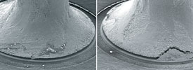
Board and component finish selection is another selection parameter that can affect reliability and production output. Component finishes containing lead or bismuth can cause fillet lifting (Figure 1). Most component leads are available in pure tin format with a nickel barrier over copper. This is done to prevent tin whisker growth. Tin is an easy metal finish to solder to and has a reasonable shelf life if stored under controlled conditions.
Board finishes of matte tin give the best soldering results. Gold over nickel finishes and immersion silver, however, also solder well. Bare copper OSP with no-clean fluxes give the lowest wetting values during wetting balance tests. These boards, with thickness in excess of 2,36 mm, are proving difficult to solder with lead-free solders. Although more difficult, the soldering of thicker boards is not impossible, and may require modification of wave process parameters or flux chemistry to obtain the desired hole fill.
In soldering of bare copper OSP with lead-free alloys, such as SnAgCu, the following can be tried to improve hole fill:
* Reduce conveyor speed to increase solder contact time.
* Increase flux volume applied, reduce air knife pressure.
* Use more active flux systems such as water washables or higher solids no-clean fluxes.
* Increase solder pump rpm to push molten solder higher into the barrel.
* Increase solder pot temperature by 10°C.
* Use fluxes with higher solids content. higher acid values.
Many of the above points can be applied in situations where hole fill is not adequate. They apply to lead-free and leaded wave systems. The main concern with lead-free wave soldering is the potential increase in soldering defects. These defects can cause increases in a poorly optimised lead-free wave soldering:
* Non-wetting.
* Insufficient solder.
* De-wetting.
* Icicling.
* Cold solder joints.
* Grainy joints.
* Blow holes.
* Solder balls.
* Fillet lifting.
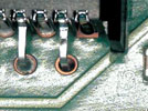
The most common defects are insufficient solder, skips, a lack of hole fill and grainy joints. These defects are caused by a variety of issues, but with lead-free alloys and their reduced wetting potential, coupled with higher pot temperatures, the flux selection will make the most difference in reducing their occurrence. If the problem persists, slowing down the conveyor speed to increase solder contact will increase hole fill (Figure 2).
Optimising wave solder for lead-free
Taking all of these points into consideration, how does an engineer optimise their wave solder machine? The process can be summarised as follows:
* Make the equipment lead-free compatible, and talk to the supplier.
* Identify lead-free components and boards, and work closely with parts suppliers.
* Select a lead-free solder; SAC305, Sn/Cu, or other compatible options.
* Choose the flux chemistry, VOC-free flux preferred, designed for lead-free.
* Run a design of experiment.
* Determine the best set of parameters to achieve maximum wetting and hole fill.
* Set up a lead-free wave and define the process and statistical limits.
* Ensure lead-free materials are segregated from leaded ones.
* Set up compatible hand soldering and rework processes.
* Cleaning process parameters, if water washable.
In some cases, flux residues tend to polymerise into a harder crystalline material that can affect probe testing, and also the cleanability of the residues. This will be very much chemistry dependent, however, higher solder temperatures and longer contact times play a role.
At times, if a cleaning agent is used in water wash systems, it may require changing to alternatives designed for lead-free cleaning. Many solder companies already have assessed the cleaning effectiveness of their new fluxes with manufacturers of cleaning agents. Asking for their recommendation is the first step.
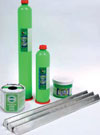
During the initial installation of a lead-free wave operation, leaded and lead-free waves may be in operation. It is important to avoid cross-contamination, because lead-free solder is similar in colour to leaded 63/37. Ideally, lead-free solder bars should be supplied with a unique shape, markings, and labelling to avoid costly mistakes (Figure 3). The current consensus is to keep Pb levels at 0,3% maximum in the solder pot, to avoid reliability issues. It is also worth noting that the maximum lead level to qualify as a lead-free joint is 0,1% lead. This does not allow for much contamination of lead in the wave solder pot.
Segregating dross or oxides from solder pots also should be encouraged. Some companies use red or black buckets for leaded oxides, and green or white buckets for lead-free. The value of lead-free oxides is substantially more than for 63/37. Keeping them separated will ensure maximum return when sold for recycling. It is also advisable to label wave solder machines with inscriptions to avoid confusion. Soldered board identification will be required to determine which is lead-free (and which is not).
With proper care and a methodical approach, lead-free wave soldering can be accomplished reliably. Resources are available through various published papers and websites about how to achieve this confidence.
Key process requirements for reliable lead-free SMT assembly
Lead-free SMT can be achieved reliably if several process requirements are carefully implemented. The most common alloys used in lead-free SMT are Sn-Ag-Cu ones, which all have a melting range between 217 to 220°C. These alloys all melt at temperatures higher than traditional leaded solders, such as 63/37 (which has a melting point of 183°C).
Key variables summary:
* Melting temperature of the alloy;
* Flux chemistry - activation and temperature effects.
* Wetting and surface tension properties of the alloy.
* Solder balling and bridging potential increases.
* Component/board reliability.
* Compatible rework/repair.
* Compatible wave, selective soldering process.
* Quality inspection criteria;
* Cosmetic effects of flux at higher reflow temperatures;
* Nitrogen vs air;
* Pin testability of flux residues;
* Solder voids impact;
* Residue cleaning/removal process changes;
* Conformal coating and underfill materials;
* Oven maintenance and flux decomposition volumes.
The melting point of these alloys is higher, so the thermal profile also requires optimisation to avoid exposing components and boards to excessive temperatures (Figure 4). The peak temperature range for SAC alloys will be between 235 and 245° C, but if the boards have small thermal masses and the oven has sufficient heating zones, temperatures as low as 229°C have been used.
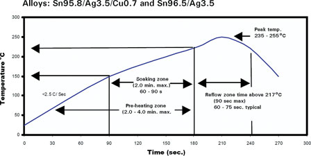
Typical reflow profile used with lead-free SAC and SnAg alloys
The flux chemistry used in lead-free pastes is designed to minimise several of the issues associated with higher reflow temperatures. Higher temperature issues can range from increased paste slump to charring of the residues. Solder paste manufacturers are using chemicals that offer good hot slump resistance and activation at higher preheats and peak reflow temperatures.
Lower wetting speeds associated with alternative lead-free solders make flux activation a critical factor in paste performance. No-clean and water-washable solder pastes are being designed not to require nitrogen reflow, and can produce reliable solder connections with good wetting in air. Water-washable solder pastes, with their higher concentration of activators, will solder most metal finishes adequately. No-clean solder pastes will require careful selection of finishes to be soldered, as well as careful selection of a paste's attributes. Some lead-free, no-clean pastes are designed to adequately solder a variety of metal finishes. Others have difficulty with second-pass, bare copper boards, because of their lower activity. Some no-clean pastes require lower peak temperatures, while others can withstand higher temperatures without charring or polymerisation.
Nitrogen will affect solder joint cosmetics, as shown in Figure 5. Solder paste reflow in air will offer brighter, more uniform solder joint surfaces. Nitrogen reflow also will enhance wetting with lead-free solders - especially on bare copper OSP surfaces. It must be noted that the vast majority of assemblers seek a solder paste that can be reflowed in air, so many lead-free chemistries are being developed with this in mind.
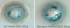
A test (shown in Figure 5) was achieved by printing lead-free solder paste on a white ceramic substrate, then reflowing one in air, and the other in nitrogen. Although the surfaces look dramatically different, this is only a surface reaction.
Selecting the best lead-free solder paste for the SMT process will be a critical variable, and the following can be used as a guide in the selection process:
* Print speed.
* Abandon time.
* Stencil life.
* Tack life.
* Solder ball test.
* Slump test.
* Spread test.
* Reflow window.
* Voiding potential.
* Double-reflow window.
* Cleanability.
* Pin testability.
It is unnecessary to repeat these tests in-house. Often, a good solder paste manufacturer will make the information available to the user. If the paste is chosen with care, and the SMT process is optimised, the lead-free transition will be achievable without jeopardising reliability and product yields. Common defects associated with lead-free include:
* Off-pad solder.
* Mid-chip solder balling.
* Tombstoning.
* Bridging (shorts) on fine-pitch QFP leads.
* Open joints.
* Non-wetting.
* Dewetting.
* Cold solder joints.
* Voids.
These defects can be avoided in a properly optimised process with a lead-free solder paste designed to provide adequate wetting, low slumping and low voiding with lead-free alloys.
Lead-free solders, because of their reduced wetting, will at times not completely wet the pad. This will be affected by flux activity and the use of nitrogen in reflow. Some assemblers, however, are modifying stencils to have less of an aperture reduction. This requires a solder paste with excellent hot slump properties to avoid bridging and solder balls. Other assemblers are seeking modifications to pad design. In many cases, this is not considered an issue.
Developing a lead-free SMT process requires good planning and a close working relationship with all suppliers. A team approach and proper training are essential for reliable lead-free integration - especially where dual systems (leaded and lead-free) are present.
| Tel: | +27 11 704 3020 |
| Email: | [email protected] |
| www: | www.ama-sa.co.za |
| Articles: | More information and articles about Allan McKinnon & Associates |


© Technews Publishing (Pty) Ltd | All Rights Reserved
 printer friendly version