


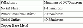
Ref: z2816201m
Removal of lead (Pb) from finished integrated circuit (IC) packages and the assembly processes used to make them is an ongoing effort by many manufacturers. The removal of Pb in consumer paint products and gasoline has already been undertaken. Many evaluations are underway now in the electronics manufacturing industry to find a suitable substitute for Sn/Pb solder.
The goal of this study was to evaluate a totally Pb-free solder joint formed by using TI 4-layer Ni/Pd finish IC components, Castin Pb-free solder paste, and Entek Plus organic solderability preservative (OSP) as the PWB surface finish. Mechanical tests performed included contact angle measurements and lead pull. Temperature cycle testing was performed to evaluate the package integrity after cycling through temperature extremes. The wetting balance test was used as a tool to determine the solder wetting time for the individual IC components.
The results show that the contact angles do increase with Ni/Pd and Ni/Pd/Au finishes. However, Ni/Pd and Ni/Pd/Au finishes achieve equivalent or better lead pull and temperature cycle testing results versus Sn/Pb. This indicates that any difference in performance of the three different lead finishes is visual only. By using TI 4-layer Ni/Pd finished IC components, AIM Castin Pb-free solder paste and the Entek Plus PWB surface finish it is now possible to achieve a totally Pb-free solder joint.
The toxicological effects of lead (Pb) have brought about the reduction or elimination of Pb use in many major industries. Historically, this has been fostered by legislation. Today the majority of passenger vehicles in the US operate on lead-free fuel. The use of Pb has been banned in the manufacture of paint due to the health hazard posed to children[1]. Although the use of Pb in the electronics industry accounts for only 7% of the total Pb consumption in the US, pressure is mounting to remove Pb from electronic manufacturing processes[2].
In response to the concern over the Pb used in electronic products and manufacturing environments, much work is ongoing to find acceptable Pb-free solder paste for surface mount operations and bar solder for wave soldering operations. Elimination of Pb in the solder used to attach electronic components to the circuit board addresses only a segment of the entire electronic assembly. Solder used to coat the Cu land patterns on the PCB as well as the solder on the component leads must be removed to have a truly Pb-free system.
In 1989 Texas Instruments introduced a revolutionary new leadframe finish for integrated circuit (IC) components. Comprised of four layers of nickel (Ni) and palladium (Pd) this system uses a very thin layer of Pd on the top surface to protect the underlying pure Ni layer from oxidation (Figure 1)[3].
By using TI's 4-layer Ni/Pd finished leadframes, Pb can be eliminated from the semiconductor manufacturing flow. There is no Pb used in the manufacture of the leadframe. Serendipitously, cyanide has been removed from the leadframe manufacturing process by elimination of the silver spot previously plated to provide a wire bonding surface. At the IC assembly/test site the costly and time-consuming operation of solder plating after plastic encapsulation is eliminated. With use of palladium-finished IC components, a Pb-free solder paste, and a non-Sn/Pb coating on the Cu land patterns the IC user can completely eliminate Pb from the board mount process and finished printed circuit board (PCB) assemblies.
Experimental design
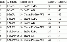
This evaluation was performed using the test matrix outlined in Table 1.
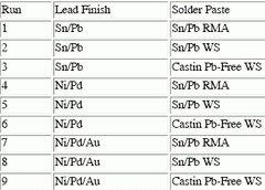
The IC test vehicle used for this evaluation was a 14 pin small outline integrated circuit (SOIC). The device housed in the 14 pin SOIC package was an HC373. Components were built using three different leadframe finishes. Units were built using the TI 4-layer Ni/Pd finish and a gold (Au) flashed version of the TI 4-layer Ni/Pd finish. The Au flashed finish uses the 4-layer structure in Figure 1 with an ultra thin layer (c. 50 angstroms) of Au on top of the Pd. This version of the Pd finish has been introduced into the market in Japan. For the Sn/Pb finish components HC373 devices in the 14 pin SOIC package built by another IC manufacturer were procured.
The solder pastes included in the study were a widely-used 63/37 RMA paste, a widely used 63/37 water-soluble paste, and AIM Castin water soluble Pb-free alloy. The AIM Castin paste is a commercially-available water soluble Pb-free alloy containing tin, silver, copper and antimony. Eutectic Sn/Pb RMA type pastes were predominant in the market until the early 1990s when IC users began converting to water soluble and no-clean type Sn/Pb pastes. The intent of this choice of pastes was to compare performance of the three finishes using the conventional RMA Sn/Pb alloy, a contemporary water soluble Sn/Pb alloy and a recently introduced commercially available Pb-free alloy.
The printed circuit board's Cu land patterns were protected with Entek Plus CU-106A. This coating is an organic material (substituted benzimidazole) used to preserve the solderability of Cu through multiple soldering operations. During SMT reflow most of the organic solderability protector (OSP) is displaced by the wetted solder and becomes a negligible constituent of the solder paste residue. Some of the OSP (<25%) volatilises at reflow temperatures.
Performance measures and results
In this study we used visual, mechanical, and reliability test methods to classify the performance of the various solder joints. The various methods used and results obtained are shown below.
Contact angle
The definition of contact angle used herein is the angle formed by the tangent to the backside of the lead and the tangent to the solder fillet at the point of contact of the lead with the fillet (Figure 2). Contact angle is typically measured by performing a cross-section on the lead of interest. Once the cross-section is available, the contact angle measurement can be taken.
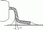
In general, lower contact angles are considered to indicate a soldering condition that has produced good results and higher contact angles indicate either a situation where the wetting rate has been decreased or where the equilibrium wetting point has changed. Contact angle can also be affected by the geometries of the soldered surfaces (relevant to the surface tension of the solder) and by the volume of solder present.
One problem with this technique is that it is subjective in the interpretation of how small the contact angle should be to indicate a good joint. Several values have been put forth. Howard Manko in 'Solders and Soldering', states: "M, the marginal limit of the dihedral angle, is usually arbitrarily set at 75° or less in the case where extremely high quality is required"[4]. This is confirmed by an electronic industry solderability test RS 178 of the EIA which contains the following statement: "Good wetting is characterised by a contact angle between the lead and the edge of the solder of 75° or less".
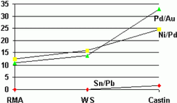
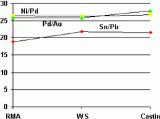
For this experiment, board-mounted IC units from each of the nine groups were cross-sectioned and the contact angle was measured and recorded. Table 2 shows the contact angle data for each of the experimental groups.
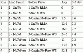
The contact angle data in Table 2 is shown graphically in Figure 3.
This matrix design of this experiment allows for calculation of an Analysis of Variance (ANOVA) table for the two factors evaluated. The ANOVA table calculations compute the variance in the contact angle data seen between the three different lead finishes and the three different solder pastes. From this information we can assign percent contributions of each factor to that variance. Results of the ANOVA calculations are shown in Table 3.
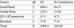
The ANOVA calculations indicate that the lead finish has the strongest impact on contact angle. The solder paste had a lesser impact on contact angle variance with the interaction of the two factors being nearly negligible. The highest contact angle measured was 40° thus all of the groups exhibited wetting angles considered to be acceptable based on the criteria put forth by Manko. In comparing the different groups the data indicates that both the Ni/Pd and the Pd/Au lead finishes exhibited higher contact angles than the Sn/Pb finished components.
Previous work has shown similar results on contact angle measurements of Pd components. Previous data has also shown that palladium finish components exhibit greater sensitivity to changes in the solder paste compared to solder plated components. Mechanical testing has shown, however, that the strength of the solder joint is equivalent, independent of the lead finish used[5]. This difference in contact angle between the lead finishes and solder pastes has previously been shown to be a visual issue only and does not negatively impact the mechanical strength of the solder joint. Actual photos of cross-sectioned units for the three different lead finishes mounted with the Castin Pb-free solder paste are shown in Figures 4-6.

Lead pull
Lead pull testing was performed to determine the mechanical force needed to pull an individual IC lead from the PCB land pattern after soldering. First, in order to allow for access to an individual lead on the PCB the leads are cut near to the package body. Next with the leads separated from the package body the PCB is fastened in a test fixture. Then the lead is pulled until it separates from the PCB. The force needed to pull the lead from the PCB is measured and recorded.
The lead pull data (Figure 7) shows that the mechanical strength of the solder joint is equivalent independent of the solder paste selection for both Ni/Pd and Ni/Pd/Au finishes. The lead pull test data indicates that mechanical strength of the joints is worse for the Sn/Pb finish components versus the Ni/Pd and Ni/Pd/Au finishes. In all cases the mechanical strength of the solder joints made with the Castin Pb-free solder paste was equivalent or better than that of the joints made with the conventional RMA and water-soluble pastes.
Lead pull failure modes
After the leads were pulled from the PCBs on the various groups above, the components and PCBs were inspected to determine where the failure actually occurred. Each unit was categorised into one of two different failure modes. Category 1 was indicated when the solder was pulled completely from the pad. This mode of failure would indicate the wetting to the lead to be stronger than the wetting to the pad. Category 2 was used when solder was left on both the lead and the pad. This failure mode would indicate that the yielding occurred within the solder itself. Results are shown in Table 4.
The data indicates that for the Sn/Pb components the predominant failure mode was within the solder itself with solder being left on both the lead and the pad. For the Ni/Pd and Ni/Pd/Au finish components the solder was pulled completely from the pad.
Temperature cycle testing
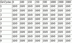
Temperature cycle testing of IC components is a reliability test performed to determine the package integrity after repeated exposure to temperature extremes. These temperature ranges are intended to simulate worst case operating duty cycles. For this experiment 10 board-mounted units from each group were exposed to a temp cycle range of -65°C to +150°C for 3000 cycles. The units were removed from the temp cycle chamber at various read points and tested electrically. The results in Table 5 show that all of the lead finish and solder paste combinations passed electrical test out to 3000 cycles.
Additional units from each group were exposed to the temperature cycle testing above for mechanical cross-sections. One unit from each of the nine variations was removed from the chamber after 50, 100, and 250 cycles. Each unit was cross-sectioned and 10 leads were inspected looking for cracks in the solder joint. Fresh board mounted units (no temp cycle exposure) were also sectioned and inspected to provide a baseline comparison. Cross-section results are shown in Table 6.
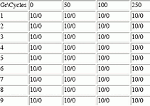
The cross-section results show that there were no cracks noted in any of the joints after temperature cycling out to 250 cycles.
Wetting balance test results
The wetting balance test (sometimes called a meniscograph) is a method used by some to test wettability of IC leads. The wetting balance test is classified in ANSI/J-STD-002 as a 'Test without established Accept/Reject Criterion'. This test method is recommended for engineering evaluations only and not as a production pass/fail monitor.
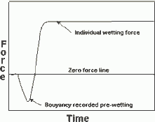
The wetting balance test measures the forces imposed by the molten solder upon the test specimen as the specimen is dipped into and held in the solder bath. This wetting force is measured as a function of time and plotted. A typical wetting balance curve is shown in Figure 8. Initially, the force is negative indicating that the solder has not yet begun to wet to the specimen and, in fact, shows a buoyancy effect. The force exerted by the solder approaches zero as the solder begins to wet to the specimen. One commonly used performance measure is the time to cross the zero axis of wetting force. This point indicates the transition from non-wetting (F<0) to wetting (F>0)[5].
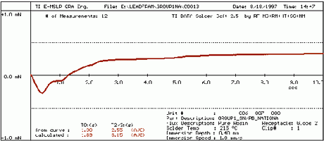
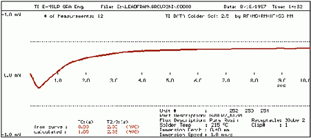
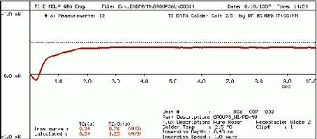
The wetting balance test was used to compare wetting performance of the three different lead finishes used in this experiment. Samples of each lead finish were tested and the wetting balance curve for the combined readings was plotted. Figures 9-11 show the curves for Sn/Pb, Ni/Pd, and Ni/Pd/Au respectively. For this test, eutectic 60/40 Sn/Pb solder was used. The flux used was RMA.
Average time to cross the Zero axis was calculated and recorded for each lead finish. Results are shown in Table 7.
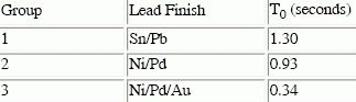
From the wetting balance results it can be seen that the Ni/Pd and the Ni/Pd/Au finishes both crossed the Zero axis more quickly than the Sn/Pb with the Ni/Pd/Au giving the fastest time to cross Zero. This result would be expected in the wetting balance test as the additional gold on the surface of the Pd wets very quickly.
TI originally introduced the Ni/Pd leadframe finish into the market in 1989. The Ni/Pd/Au finish has recently been introduced in Japan as an alternative to the TI Ni/Pd finish. The data in this report shows that there is no difference in actual board mount performance of the Ni/Pd finish and the Ni/Pd/Au finish units. The only noted difference was the slight improvement in wetting balance by addition of the Au flash. Texas Instruments has no intention of adding Au flash to the original Ni/Pd finish. Additional cost for the Au layer along with possible reliability problems associated with gold embrittlement negate any perceived improvement in the final product.
Texas Instruments is now evaluating (added July 2000) the performance of a NiPdAu lead finish with various Pb-free solder pastes being considered by our customer base and the industry in general (NEMI, ITRI, IPC). The gold flash may help to flatten any differences in solderability and wetting balance performance seen with the different Pb-free solder alloys. The version of NiPdAu that is under consideration addresses the gold embrittlement issue by recognising it and minimising the gold content in the finish. Texas Instruments has also received customer inputs requesting NiPdAu finish.
Results summary
* Contact angle data for Ni/Pd and Ni/Pd/Au finish components was higher than for Sn/Pb components for all types of solder pastes evaluated. Differences in contact angle proved to be a cosmetic issue only and did not correlate to any difference in reliability or mechanical strength of the joints.
* Lead pull data was lower for Sn/Pb finish components compared to Ni/Pd and Ni/Pd/Au for all types of solder pastes evaluated. Data was essentially equivalent for Ni/Pd and Ni/Pd/Au finished components.
* Lead pull failure mode analysis showed the Sn/Pb components failed within the solder. In most cases with Ni/Pd and Ni/Pd/Au components the solder was pulled completely from the pad.
* Temperature cycle testing of the three different lead finish components with each solder paste showed no failures out to 3000 cycles. The temperature cycle range was -65°C to +150° C.
* Cross-sections of temp cycled units showed no cracks in the solder joints out to 250 temperature cycles.
* Wetting balance test results showed that the Sn/Pb components took longer to pass the T0 line that the Ni/Pd or the Ni/Pd/Au finished components. The gold flash on the Ni/Pd/Au components improved wetting performance as measured by time to cross zero.
Acknowledgment:
This paper published in the March 1998 issue of Surface Mount Technology magazine. The authors wish to recognise the following employees of Texas Instruments for their professional assistance: Terrill Sallee of TI Sherman for PCB design and surface mount assembly support; Bernhard Lange and Kay Haulick for lead pull and wetting balance testing.
The authors wish to recognise the following for support with materials and technical information:
Marcia Vincent of AIM Products for supplying the Castin Pb-free solder paste; Joseph DeBiase of Enthone-OMI for technical information about Entek Plus organic solderability preservative (OSP).
References
[1] Napp, Dr. Duane, 'NCMS Lead-Free Electronic Interconnect Program', presented at Surface Mount International Conference, San Jose, California, 28 August-1 September, 1994.
[2] Kwoka, Mark A. And Foster, Dawn M., 'Lead Finish Comparison of Lead-Free Solders versus Eutectic Solder', presented at Surface Mount International Conference, San Jose, California, 28 August-1 September, 1994.
[3] Romm, Douglas W., 'Palladium Lead Finish User's Manual', September 1994.
[4] Manko, Howard, 'Solders and Soldering', pp. 254-257, 1964.
[5] Romm, Douglas W. and McLellan, Neil, 'Evaluation of Water Soluble and No-Clean Solder Pastes with Sn/Pb and Palladium Plated IC Devices', Surface Mount Technology, January 1993.
[6] Tummala, Rao R. and Rymaszewski, Eugene J., 'Microelectronics Packaging Handbook', pp. 837- 838.


© Technews Publishing (Pty) Ltd | All Rights Reserved
 printer friendly version