


Following the EC's directive to ban lead from electronic goods, there has been much progress in the move towards lead-free soldering technology. New alloys are being developed, and in general, their melting point is increased. Tin (Sn)-copper (Cu) (227°C), tin-silver (Ag)(221°C) or tin-silver-copper (217°C) are mainly used, whereby the eutectic behaviour needs to be kept in mind. Occasionally bismuth (Bi) is added to further reduce the melting point.
These alloys are critical, since minor contamination (the other solder on a PCB, or lead-containing connectors of components) can reduce the melting point dramatically and may cause quality and stability problems. The use of lead-free solder downgrades the process ability because of lower wetting and flow behaviour. This can only be solved by the use of improved fluxes.
Compared to lead-containing solder, lead-free solder joints appear dull and additionally, are temperature-sensitive during hardening. An increase of process temperature should be avoided due to longer cooling times that may cause micro-cracks. Soldering with higher temperatures can result in black layers on the solder tip that make them unwettable and cause early fallout (charred flux, oxidised tin, tin-iron-fusion). Thus, new materials like lead-free alloys demand new tools.
Requirements on hand-operated soldering tools
Due to higher melting points, working with lead-free solder requires:
* Tools with higher power and optimised temperature control.
* Tools with better thermal conductivity, to bring as much heat to the tip without loss.
* Optimised tip selection. Shorter and thicker tips are preferable to transfer the required heat into the solder joint without increasing the process temperature. Thermal stress on components and PCBs is reduced and the solder tip avoids damage (better lifetime and wettability).
* Cost reduction of wear parts.
Due to the higher tin content, lead-free solder causes shorter tip lifetime (due to iron leaching). In Weller's system, since the high-value heater/sensor is separated from the tip, it is only the tip that needs to be changed for wear. Weller's 'LF' (lead-free) tips additionally have an optimised thicker layer of iron. This results in higher lifetime and still ensures ideal heat transfer.
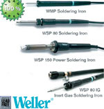
Weller irons
Weller offers a range of soldering irons for lead-free. The WMP and WSP are adjustable to particular solder tasks. These adjustments can be calibrated and audited according to ISO standards.
The WMP soldering iron is ergonomically designed - very short grip to tip distance - and efficient. The WSP 80 is a proven tool for lead free soldering in production and repair. It is ideal for production lines with continuous use. The WSP 150 is the tool for lead free solder tasks with high power demands. The large thermal capacity of the tip enables continuous working. It has increased temperature range up to 550°C. The WSP 80 IG inert gas soldering iron delivers 80 W for oxide-free lead free soldering.
Weller's hints for soldering
* For rework and repair use the same alloy that is used for the production of the boards.
* Select the working temperature as low as possible.
* Choose the largest possible tip shape for your task. Rule of thumb: about the size of the solder pad.
* Note that extensive heat transmission between tip and solder joint through a well-wetted tip.
* Soldering in an inert gas environment increases the flow behaviour and reduces the flux need; so do not use more flux than needed.
* Work with soldering tools that offer high power and a perfect thermal transfer.
* Use an intelligent soldering station with optimised temperature control and setback function to reduce the tip temperature when not in use.
* Preheat the boards with heating plates before repairing to reduce the soldering time.
* It is recommended that sufficient tests be undertaken and a detailed flow chart be set-up to detail the steps to follow in the changeover to lead-free.
Care of the soldering tip
* Clean the tip on a watery swamp (not dry nor wet) and use distilled water.
* Switch off the station during longer working breaks or use the Weller setback function.
* Add sufficient tin to the tip before placing the iron into the stand.
* Unwettable tips can be reactivated with Weller Tip-Activator.
* Use the lowest possible tip temperature.
* Use special tips for applications with drag drop (GW-Gull Wing or KN-Knife tips).
* Apply the tin directly to the solder joint not the tip.
* If possible avoid the use of high activated flux.
* Change the tips with the appropriate changing tool.
* Apply as low a force as possible onto the tip.
* Black layers of oxidised tips can be softly removed with steel or aluminium wool.
| Tel: | +27 11 704 3020 |
| Email: | info@testerion.co.za |
| www: | www.ama-sa.co.za |
| Articles: | More information and articles about Allan McKinnon & Associates |


© Technews Publishing (Pty) Ltd | All Rights Reserved
 printer friendly version