26 July 2006Manufacturing / Production Technology, Hardware & Services
Soldering is based on the ability of different metals to dissolve or diffuse into each other and to cause an electrical connection at lowest resistance and mechanical fixing. Flux is used to dissolve metal-oxygen layers on the surface of the different metals being connected with each other due to the dissolving of the tin into them.
Soldering tips
A soldering tip has two major tasks. The first is to transfer thermal energy with as low a loss as possible, and secondly, to carry the solder on the joint in combination with flux. Due to physics, the tip turns out to be a wearing part. And these tasks have to be done in combination with achieving long lifetime and at lowest cost.
To achieve excellent thermal conductivity, a soldering tip consists of a copper core (silver would be better, but is much more expensive).
The wettability of copper with solder tin is extremely good, which means the solubility of copper in solder tin is extremely high, causing the tip to be quickly consumed. The tip must be wettable to properly carry the heat and the tin on the soldering joint. Iron is also wettable with tin, but the solubility is far less. Unfortunately iron has a very low thermal conductivity and hinders thermal flow. The thicker the iron layer, the lower the heat transfer from the tip towards the soldering joint. The thinner the iron layer, the shorter the lifetime due to the solubility of iron in tin. Using other materials that are not soluble in tin will cause a non-wettable tip and poor soldering results.
Heating tips to high temperatures
The aggressiveness of the solubility of iron into tin increases with rising temperature. So also, the mechanical resistance of the tip's iron layer is reduced. When soldering, the tip is somehow always touching some part of the component and is in contact with the aggressive tin. Now, with lead-free soldering, the content of the tin in the solder is increased by 35%. This results in a 35% more aggressive solder towards the iron layer, simply causing reduction in life.
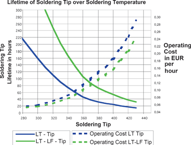
Now, standard tips have an average iron layer of 200 μm depending on the geometrical form. Weller's new LF tips carry an optimised layer of twice as much iron. More iron would cause a lower heat transfer and hinder the soldering process. Influence of the temperature to the lifetime and iron layer can be seen in Figure 1.
Figure 1. The graph shows that the LT-LF soldering tips provide a cost reduction and that the main influence to tip lifetime is the soldering temperature
A general recommendation is to use a tip as large as possible, and if necessary, to improve the process by using a thinner solder-wire. For lead-free solder, the adjusted soldering temperature at the station should be in the range of 340-360°C, depending on the geometry of the tip. For further enhancement of tip lifetime 'Stop+Go' stands should be used.
Collaboration is now critical RS South Africa
Manufacturing / Production Technology, Hardware & Services
The message emerging from RS Connect is clear: Organisations can no longer rely on internal optimisation alone to secure performance. Competitive advantage is increasingly being determined by the strength of external relationships, shared capability and coordinated action across value chains.
Read more...Disruption is the new normal. Effortless is the new competitive advantage. Seven Labs Technology
Manufacturing / Production Technology, Hardware & Services
Global supply chains have been under pressure for years. The manufacturers still standing are the ones who stopped waiting for normal to return, and started building something better.
Read more...World-first 016008 mm component placement
Manufacturing / Production Technology, Hardware & Services
Fuji has achieved the world’s first placement of 016008 mm (0,16 x 0,08 mm or 006 x 003 inches) size components on printed circuit boards with its SMT pick and place machine, NXTR.
Read more...Lifecycle and obsolescence: Protecting electronics through process Production Logix
Manufacturing / Production Technology, Hardware & Services
At Production Logix, we believe longevity is not accidental. It is engineered through early visibility, structured response, and disciplined execution, in partnership with our OEM customers.
Read more...Maximising squeegee quality and durability Testerion
Manufacturing / Production Technology, Hardware & Services
Transition Automation has announced two new product advancements designed to improve SMT printing performance and extend squeegee life: laser-enhanced Permalex bonding and integrated edge protectors.
Read more...NeoDen ND2 PCB screen printer ZETECH ONE
Manufacturing / Production Technology, Hardware & Services
The NeoDen ND2 PCB screen printing machine is a fully automatic stencil printer designed to deliver precise and consistent solder paste application in modern SMT production environments.
Read more...Understanding the BGA rework process Techmet
Manufacturing / Production Technology, Hardware & Services
BGA rework is a highly technical process that involves removing the faulty component, preparing the circuit board, and installing a new or repaired device, while maintaining the integrity of the printed circuit board.
Read more...Flexible three-process reflow soldering system Truth Electronic Manufacturing
Manufacturing / Production Technology, Hardware & Services
By combining multiple soldering technologies within a single system, the Vision TripleX system enables manufacturers to adapt easily to different assembly requirements, board designs, and production volumes.
Read more...Inline vapour phase soldering for high-volume production MyKay Tronics
Manufacturing / Production Technology, Hardware & Services
The VP2200-100 vacuum inline vapour phase soldering system from ASSCON is designed for fully automated, high-volume electronics manufacturing where process consistency and solder joint quality are critical.
Read more...Global electronics solutions since 1964 IMP Electronics Solutions
Manufacturing / Production Technology, Hardware & Services
Over more than six decades, IMP Electronics Solutions has built a reputation for technical expertise, reliable supply chains, and strong partnerships with both customers and manufacturing partners.
While every effort has been made to ensure the accuracy of the information contained herein, the publisher and its agents cannot be held responsible for any errors contained, or any loss incurred as a result. Articles published do not necessarily reflect the views of the publishers. The editor reserves the right to alter or cut copy. Articles submitted are deemed to have been cleared for publication. Advertisements and company contact details are published as provided by the advertiser. Technews Publishing (Pty) Ltd cannot be held responsible for the accuracy or veracity of supplied material.


 printer friendly version