


Production soldering with lead-free alloys, driven by environmental, health, and legislative concerns, is in the electronics industry's near future. Process development is certainly ongoing.
The European 'IDEALS' consortium and others have conducted investigative studies on Pb-free wave soldering, and have concluded that Pb-free soldering is technologically possible, but a number of implementation issues must be addressed. For example, the introduction of VOC-free flux technology will significantly impact the Pb-free soldering process, and the soldering process in general will have to be modified to accommodate the requisite higher soldering temperatures. Taguchi methods and statistic process control are an effective way to approach and evaluate Pb-free process development in wave soldering, to determine the most essential control parameters in order to achieve the optimum process set-up for an individual application.
Taguchi method summarised
The recognised analysis approach known as the Taguchi method integrates an innovative approach to quality with traditional methods for the design of experiments, in which a series of interrelated techniques are developed that in concert help minimise unwanted variability, reduce production waste, and provide greater customer satisfaction.
The Taguchi approach for reducing variation in production is a two-step process:
1. Manufacture the product in the best manner most of the time (less deviation from the target).
2. Produce all products as identically as possible (less variation between the products).
The Taguchi method employs experiments using a specially constructed 'orthogonal array' table to affect the design process, such that quality is built into a product during its design stage. An orthorgonal array is an experimental design constructed to allow a mathematically independent assessment of the effect of the different factors affecting the experiment.
Preparation
The preparation for a Taguchi experiment begins with a 'brainstorming' session, in which a team of participants from different disciplines establish clear statements of problems, objectives, desired output characteristics and method of measurement used to design the appropriate experiment. Afterwards, all the process parameters are identified. Relevant factors affecting the outcome are defined thus:
1. Controllable factors:
C1 = factors that contribute significantly to the process and can be directly controlled; and C2 = factors for which we need to stop the process if we change them.
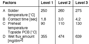
In our experiment, three C1 factors were selected: B = contact time; C = preheat temperature; and D = flux amount.
The solder temperature is a C2 factor due to the time it takes to increase/decrease the temperature.
2. Noise factors:
Noise factors are the product of process variables that affect variation, but are impossible or cost-ineffective to control. Examples of noise are changes in environment temperature, humidity, dust, etc, during the production/experiment.
For practical reasons, there was no 'noise' element factored into the experiment. The main goal of this experiment was to estimate the contribution of the individual quality-influencing factors. Other experiments need to be conducted to quantify their response to noise in the process. Finally, a selection had to be made as to which output characteristics we wanted to measure. There were two criteria selected:
1. The number of pins without bridges.
2. Qualification of through-hole fill.
Experiment layout and design
In contrast to other methodologies, which use mostly one-factor-at-a-time studies to identify controllable parameters, this experiment uses an L9 orthogonal array. In only nine experimental runs, four factors at three levels are investigated, as shown in Table 1. The layout of the array is shown in Tables 4 and 5.
Output characteristics
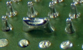
A proper experiment set-up is required in order to obtain the most reliable data. For example, the range of control parameters must be as extreme as practical in order to make problems (in this case bridging and bad hole penetration) apparent. To quantify the effect of bridging, the number of soldered pins without bridges were counted.
Each board had 200 pins, so the maximum score could only be 200.
The score for the component in Figure 1 was '6', because six pins do not exhibit bridging, whereas the others do.
For the effects of through-hole penetration, each hole filled with solder was marked as shown in Figure 2:
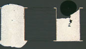
A total of 4662 points were the maximum achievable for each board.
Materials used in the experiment
The Pb-free Alloy
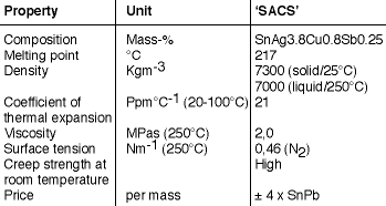
The most commonly used Pb-free alloys for wave soldering are SnCu and SnAgCu. SnCu is one of the least expensive Pb-free alloys available. This alloy has, however, a high melting point (227°C), and its mechanical properties are poor compared to other Pb-free alloys.
SnAgCu is an improvement over the basic SnAg. SnAg3.8Cu0.7 forms joints of higher reliability and the solderability is better than SnAg and SnCu. The addition of antimony, Sb (0,25-0,5%) provides added thermal resistance. The strength of the alloy increases by the intermetallic structures of antimony with silver and copper. However, there is some concern regarding the toxicity of Sb, although toxic Sb-oxides are generated at temperatures above 600°C.
SnAg3.8Cu0.7Sb0.25 (SACS), with a melting point of 217°C, is used in our experiment (see Table 2).
Board finish
The organic solderability preservative (OSP), Entek Plus Cu-106A, a high performance copper protective coating, that selectively protects and maintains solderability of through-holes, was selected for this test board. Earlier studies demonstrated that SnAgCu is compatible with OSP finishes.
OSP is a replacement for hot air levelling (HASL) and other metallic printed circuit board finishes. With higher preheat settings, the thin organic coating (thickness 0,2-0,5 µm) loses activity. The compatibility of OSP with water-soluble fluxes is excellent. Acids and solvents contained within the flux quickly dissolve the thin OSP coating, which becomes part of the flux, and volatilises when the molten solder contacts the board.
The flux
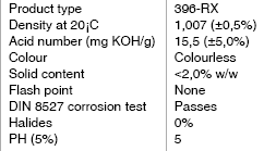
The flux selected for this test was 396-RX synthetic VOC-free with less than 2% solids (physical properties shown in Table 3). This halide free, low residue flux was selected due to its good solderability on copper surfaces. 396-RX is also very effective in preventing bridging. Preheat for this flux, measured in topside temperatures, may range from 100 to 112°C, depending on the configuration of the assembly to be soldered.
Flux application
Of the flux application technologies available, a nozzlespray fluxer is the best type to apply an appropriate layer to the board. Flux droplet size can be controlled with adjustment to air atomising pressure control. With VOC-free fluxes, it is important to achieve the finest (smallest) droplets possible in order to achieve good through-hole penetration and successful volatilisation of the water film. Therefore, a water-based flux should have carefully formulated surface properties, yielding a smooth interface with both the metallic and nonmetallic surfaces.
The nozzle fluxer allows the user to control the amount of flux very precisely, from approximately 300 mg/dm² to 750 mg/dm² (wet flux). The maximum is 750 mg/dm², because beyond this point excess flux begins dripping off the board.
Test board
Test board dimensions were 160 x 100 x 1,6 mm. Material was FR4 with copper double side plated through-holes. The connectors have 10 pins, double row with a 0,2 μm AuNi finish.
Test results
For the test, we ran 18 boards (nine boards with one repetition) to obtain the data needed for orthogonal array analysis to achieve the following objectives:
* To estimate the contribution of individual quality influencing factors.
* To gain the best, optimum condition for the Pb-free process.
* To approximate the response of the control parameters under optimum conditions.
ANalysis Of VAriance, a statistical treatment, is used to analyse the results of the orthogonal array experiment and to determine how much each quality influencing factor has contributed. Table 4 shows the data related to bridging obtained from the experiment.
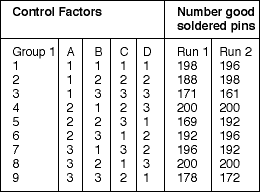
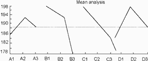
Figure 3 illustrates the incidence of bridging relative to process factors. As mentioned earlier, the higher the number, the better (200 = no bridging). Figure 3 shows that, with respect to bridging, contact time and preheater temperature affected output data the most; ie, changing one of these settings will have the most dramatic effect on the number of bridges.
Optimal settings for bridging based on experiment data were determined to be A2, B1, C1, and D2. Although the difference between A2 and A3 was very small, we selected A2 for two reasons:
1. Solder temperature of 260°C is preferred due to lower energy consumption requirements.
2. Solder temperature of 260°C causes less thermal shock to components and board material.
Figure 4 shows the impact in % of each control parameter with respect to bridging.
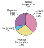
Table 5 lists the experimental results related to through-hole wetting.
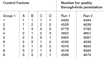
In Figure 5, once again, the higher the count, the better (4662 = a 100% good soldered board). Preheat temperature (130°C) affects the process the most, while the impact of the other factors is about equal. The experiment repetition error was found to be small for through-hole penetration.
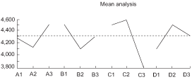
Optimal settings established for the best through-hole penetration of solder based on experiment data were A3, B1, C2, and D2.
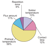
Figure 6 shows the impact in % of each control parameter related to through-hole penetration.
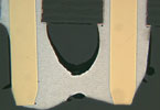
Microscopic pictures of joints
Cross sections were made of the 'SACS' solder joints of testboards from the experiment.
Discussion: Results
The impact of solder temperature is minor relative to its effect on bridging. For through-hole penetration, a higher solder temperature is better. However, this option may be limited due to potential damage to components, flux activators and board material.
Shorter contact times yielded better results for this experiment, possibly because the flux activator system was compromised at the higher preheat and solderpot temperature settings. This is typical for this type of flux under these process conditions. Other tests revealed that longer contact times could be of benefit if the flux activations system is strong enough to withstand the higher temperatures. Otherwise, contact times of 2,5 to 4 seconds are recommended.

In terms of preheater temperature, a setting of 110°C is the champ for this process. At a higher preheater temperature (130°C) the process window narrows remarkably; the OSP coating and the flux may lose activity. Pre-heating water-based VOC-free flux requires special consideration. Once the flux is applied, it is essential to improve the chemical bond between the flux and the board surface. This can be achieved by heating the flux. Consequently, at the end of the first process zone (600 mm), the temperature of the top side of the board should be approximately 70-80°C. For this test, medium-wave Calrod R-generating elements were selected. The elements provide the appropriate volume and wavelength of IR energy to initiate activity without forcing the water to boil out of the material at the start. Forced convection heating is used in the second and third zones to eliminate excess water before entering the solder waves.
It is essential to have a continuous, uniform spray pattern of flux all across the board. The finest possible droplets applied with the lowest possible air pressure setting will deliver the best result. Higher settings may cause a droplet 'bouncing' effect, rather than improved wetting of the board surface. The D2 setting was the paper champ in our experiment.
The overall paper champ for this experiment is listed as follows: A3, B1, C2, and D2.
A. Solder temperature = 275°C; to avoid thermal damage, between 265-270°C.
B. Contact time = 1,8 s.
C. Preheat temperature (topside) PCB = 110°C.
D. Wet flux volume = 474 mg/dm².
Conclusion
For Pb-free wave soldering in production volumes to be implemented successfully, the entire process must be reviewed, for it is not simply a matter of dropping new chemicals and materials into the process. This review can be facilitated, and process development expedited, by conducting a Taguchi analysis and appropriately-designed experiment. This enables the process engineer to reach a practical understanding of what will be required in his own specific application with only a small number of test runs. Although new Pb-free wave soldering processes will have a smaller process window due to higher temperatures and other materials, SPC can be a valuable tool to help the engineer remain within correct specifications and to achieve the minimum variation in the newly-developed process.
This test board used in this experiment was run on a standard (Vitronics Soltec) Delta 6622 wave soldering machine equipped with a spray-nozzle fluxer, a three stage preheater, and nitrogen, obtaining repeatable results in this Pb-free process at a conveyor speed of 2 m/min without problems. This illustrates that special or non-standard equipment or options will in most cases not be required to convert to a Pb-free process. The spray-fluxer used is capable of delivering adequate flux to the through-hole barrels. This is particularly encouraging, since foam fluxers in general will not work properly with most water-based VOC-free flux; special newly-formulated fluxes are required.
| Tel: | +27 11 609 1244 |
| Email: | zetech@zetech.co.za |
| www: | www.zetech.co.za |
| Articles: | More information and articles about Zetech One |


© Technews Publishing (Pty) Ltd | All Rights Reserved
 printer friendly version