
The world is starting to focus on tin-silver copper as the lead-free alloy of choice. This article discusses the commercially available tin-silver-copper alloys and their processing and reliability, as well as the world-wide level of acceptance, forwards and backwards compatibility, contamination issues, environmental and economic impact.
In the processing section we will present practical data on surface finish compatibility and voiding.
Background
Lead-free is here and it is happening now. The European RoHS (restriction of hazardous substances) regulations apply from 1 July 2006. Most Japanese consumer OEMs have target conversion dates in 2004. Wave solder is converting first, followed by reflow. Lead-free components are now available but there are still a lot of concerns.
Our solder reclaim plant at Altoona has identified 13 different electronic and industrial lead-free alloys which must be separated and segregated (life was much simpler with tin-lead and tin-lead-silver alloys only). The JEITA lead-free roadmap shows that many alloys are still being considered, but that tin-silver-copper is emerging as the alloy of choice in Japan in reflow (58%), wave (64%), hand solder (78%) and solder spheres (87%).
Why tin-silver-copper?
There is no direct drop-in alloy which is similar in ease of fabrication, cost, processing and properties to tin-lead. Many elements are undesirable as major components because of toxicity (mercury, cadmium, gallium) or price and availability (indium, gold, bismuth). Zinc is the only low toxicity metal that approaches lead in cost and melting point but zinc alloys are very difficult to process and the resulting solder joints are subject to corrosion. This essentially leaves us with tin and copper as the major ingredients together with silver, bismuth, indium, antimony and a slew of trace elements such as nickel and germanium used to modify crystallisation. Most of these alloys melt 20 to 40°C above the tin-lead eutectic temperature of 183°C.
Tin-silver-copper alloys in the range 3-4% silver and 0,5-1,0% Cu melt in the 217 to 220°C range, are relatively inexpensive and easy to produce and have relatively low toxicity. Ternary alloys are always cheaper to produce than quaternary or higher-order alloys.
Are we better off landfilling tin-silver-copper than tin-lead? The jury is out on this due to concerns over the environmental costs of producing tin and silver and the apparent toxicity of silver to aquatic life. The EPA and IPC are cooperating on a full lifecycle analysis which will hopefully answer these questions.
Which tin-silver-copper?
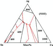
The most popular alloys proposed for electronics are 3,8% Ag 0,7% Cu (AMES), 3,9% Ag 0,6% Cu (NEMI), 4,0% Ag 0,5% Cu (widely trialled in the USA) and 3,0% Ag 0,5% Cu (proposed in Japan). All of these are in the tin-rich corner of the tin-silver copper phase diagram as shown in Figure 1.
If we look more closely around the tin corner (Figure 2) we can see that the first three alloys mentioned cluster round the eutectic melting at 217°C and the 3% silver alloy is somewhat closer to tin with a liquidus around 220°C.
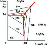
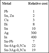
This 3% silver alloy will therefore have a slightly larger pasty range (useful in reflowing 0201 and other 'tombstoning' components) and of course a lower metals cost - about 15% less than the 4% alloy but still twice that of eutectic tin-lead (see Table 1) depending on commodity metals prices at acquisition.
Does it matter which composition you use? In most cases no; the accuracy of melting a three component alloy is 0,2%; if the bath is cooled, phases can drop out, the alloy can react with wave-solder or powder-making equipment and will dissolve metals such as copper from the boards and devices being soldered. The only alloy which you can really distinguish in production in our opinion is the 3% alloy, where lower cost and wider pasty range are balanced against a slightly higher liquidus temperature.
The tin-silver copper process
Stencil design: Lead-free paste printing must take into account the fact that the molten solder will not spread to cover pad areas left open in the print process. All alloys and surface finishes show this effect. If defects are found, the stencil design guidelines of IPC 7525 need to be modified.
Stencil wear: There is no evidence that SAC solders cause abnormal stencil wear.
Component or board overheating: It is not necessary to reflow at 260°C in many cases - on smaller boards with low thermal mass 230°C can be possible. More complex boards will require higher temperature and attention to detail on heat distribution. Careful set-up with thermal profiling of key assemblies is however critical. If reflow temperatures are uncomfortably high then nitrogen will allow them to be lowered by 10°C. Board discoloration has not been a major issue but board sag has been identified and can be remedied by using an epoxy laminate with glass transition temperature of 170°C rather than the standard 140°C.
Nitrogen cost and tombstoning: Nitrogen, as mentioned above, will 'buy you' 10°C; you can solder at a lower temperature and get a better-finish joint with less oxide but you will incur nitrogen cost (much higher in some parts of the world than others). The different rate of flux evaporation in nitrogen as opposed to air has been blamed for tombstoning in some assemblies when 0201 components are reflowed in nitrogen and the lightweight components can float on flux exudates. When specifying new reflow or wave equipment, nitrogen capability is a wise investment.
Reflow and wave equipment conversion: For really simple boards your existing reflow oven is probably fine. For complex boards you will need to use a multizone oven - seven zone and above - with integral flux management and nitrogen capability for difficult assemblies. Wave solder pots of the correct corrosion-resistant cast iron are fine, but stainless steel components are attacked by lead-free alloys over a period of a few months. All stainless steel alloys are attacked. Retrofits of specially coated stainless steel for wear-prone components are available.
Solder pot: You may well be able to use the same temperature you use with eutectic tin-lead, 250-260°C. Cast iron solder pots of the correct corrosion-resistant composition are not attacked by lead-free solders.
Dross management: Our internal study showed no statistically-significant increase in dross comparted with tin-lead even in wave soldering well above 260°C. Because of the higher value of the dross (silver and tin are much more valuable than lead but much more difficult to reclaim from dross) an integrated dross management and solder reclaim system may have a very rapid payback.
Board deformation: Already 1/3 of the US industry has switched to higher glass transition (Tg) materials - 170°C vs 140°C - for a greater margin of safety in reworking BGAs reflowed with tin-lead eutectic. These materials work fine in lead-free but take care that the time to delamination of the grade you choose - typically the T260 rating - is also improved over regular FR4. The above refers to complex boards for professional electronics. With single-sided boards for TV or other applications, even FR-2 boards can be soldered lead-free with care.
Surface finish and wetting: Lead-free HASL is available and works well. Unfortunately the metals price premium makes it much less economical than before and there is real concern about flatness and additional high temperature exposure of the board. OSP, despite the rumours, works well, even in air as long as the number of reflow cycles are limited and in nitrogen for almost unlimited cycles. It is important to distinguish some Japanese OSPs that contain a pre-flux and are only suitable for one process cycle. Tin and silver finishes perform well. Nickel-gold is fine also - but is being relegated to a more minor role as OSP, tin and silver usage increases.
Through hole reliability: With pin in paste assembly, the tin-silver-copper alloys showed far fewer defects in our study than other lead-free alloys. With wave soldering, the most dominant factor is flux composition. One major cosmetic issue is fillet lifting, minimised by managing the reflow profile and minimising the use of Pb-terminated devices that encourage an excessively wide melting range (Figures 3 and 4).

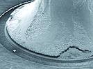
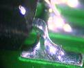
Inspection - joint appearance and voids: Because of the different crystallisation of lead-free solders, they look a little less shiny than eutectic joints due to the formation of relatively large crystals of a tin-rich phase during cooling. This is seen in all alloys and surface finishes. Voids are an issue particularly in fine-pitch BGA joints due to the high surface tension of tin-rich alloys preventing the escape of bubbles from flux solvents or microvia in pad voids. They can be minimised by careful process and materials control. Tin-silver-copper alloys and tin-lead appeared in our study to give less voids than other alloys. As seen in Figure 5, the solder has not spread to the pad edge and modification of stencils may be necessary to ensure copper coverage.
Lead-free solder flux residues: Air-reflowed boards will be tougher to clean than nitrogen-reflowed boards because of flux residue oxidation but equipment and surfactant vendors do have systems that perform well on lead-free boards.
Voids: Lead-free solders have a higher surface tension than lead-tin solders and so it is easier to trap bubbles from flux evaporation or from entrapped air due to via in pad cavities. Careful control of flux ingredients and reflow profile (especially time above liquidus) will minimise voiding.
Cross-contamination: Segregation of lead-free and lead-tin solder in processing and rework. Lead-contamination could cause reliability issues according to several studies. Lead in bismuth-containing alloys produces a low-melting phase and the reliability of lead above 0,5% in tin-silver-copper has been questioned. The issue of mixed assembly - leaded and lead-free - does not appear to generate reliability issues but there is little hard data to prove this.
Reliability under thermal cycling: We tested reliability - air to air, liquid to liquid - between 55 to 125°C. In common with other studies, we found no major difference between the alloys and surface finishes but what we did find was that large resistor components (1206) failed frequently due to joint cracking under thermal stress.
Intermetallic growth is a concern to many but has not been excessive in any of the studies that we have been involved in. Failure rates have been no higher than tin-lead.
Rework: There are real concerns over reworking BGAs and controlling heat distribution to avoid damage to the component, surrounding components and the board. Leaded components, however are fairly readily repaired using tin-silver wire which seems to be becoming the material of choice for universal rework.
Roadmap
Lead-free assemblies already represent 20% of production in Japan and are growing in the rest of the world. However, we really have not attempted to produce really complex lead-free boards with a range of component technologies and we expect that for these devices (and eventually all electronics) recycling will be the preferred route. In the RoHS regulations, lead in high-melting solders, and in servers and network infrastructure solders is exempted.

Conclusions
Tin-silver-copper alloys are a useful compromise of performance, cost, reliability and processing difficulty. They will be the leading lead-free alloys and we will all have to manage their introduction over the next three years.
There are many good references available on the Web. We particularly recommend www.metallurgy.nist.gov/phase/solder/solder.html (solder alloy phase diagrams), http://www.boulder.nist.gov/div853/lead%20free/props01.html (lead-free solder properties summary), www.ipc.org, www.nemi.org, www.ncms.org, www.lead-free.org, http://tsc.jeita.or.jp/TSC/COMMS/7_EASM/english/leadfree/data/roadmap-v21-eHP.ppt (JEITA Japanese lead-free roadmap).
For more information contact Peter Vichos, Testerion, 011 704 3020.

© Technews Publishing (Pty) Ltd | All Rights Reserved