
In embedded applications it is often needed to interact with the user by means of displaying numbers or simple texts. LED displays with seven or 14 segments per character are available at low cost and in many different sizes, however, they consume a lot of current and this restricts their use in battery powered applications. LCD modules driven by HD44780 or compatible controllers have simple interface and low power consumption, however they cost more and their dimensions are often too large to fit into small enclosures.
Bare LCD displays offer both low power consumption and small size, however their drive is usually considered non-trivial. This article aims at explaining the basic principles of twisted nematic displays and disclosing one possible method of their drive without a specialised interface circuit or microcontroller peripheral.
Principle of LCD operation
Properties of liquid crystal materials were discovered in 1888 by an Austrian botanist, F. Renitzer. These materials were not suitable for commercial use however. The first nematic crystals which retained their properties even at room temperatures were developed in the 1960s, but the real breakthrough came when cyanobiphenyl materials were discovered. These have large positive dielectric anisotropy and a strong birefringence, which makes them almost ideal for the twist cell. The most common LCD is called the twisted nematic (TN) display. This display consists of a nematic liquid crystal sandwiched between two glass plates. The inner glass surfaces are coated with a transparent metal oxide film which acts as an electrode used to apply voltages across the cells. A polymer alignment layer is placed on top of the electrodes and microscopic grooves are created in it during the manufacturing process, which force the crystal molecules to align in parallel to the grooves. A layer of polymer spacer beads is eventually applied to one of the glass plates to maintain uniform gap between the two, the plates are placed together and the edge is sealed with epoxy. A small hole is left in the epoxy and the liquid crystals are injected between the plates through this hole under a vacuum. After the hole is sealed, polarisers are applied to top and bottom surfaces of the display. In TN displays the alignment layers and polarisers are created perpendicular to each other, which forces the crystal molecules to twist by 90° under no voltage conditions - see left side of Figure 1.
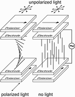
The light entering the display from the top is polarised by the top polariser and as it travels through the liquid crystals its polarisation rotates with the molecules. When it emerges, its polarisation has been changed by 90° and it passes through the bottom polariser. However, when a voltage is applied to the electrodes, the molecules will arrange vertically - see right side of Figure 1. In this case polarisation of the light passing through the liquid crystals remains unchanged and is blocked by the bottom polariser.
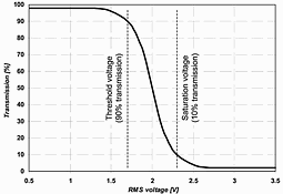
It is important to minimise DC component of the display drive signal, otherwise electrolysis process will develop and eat up the electrodes eventually. The optical effect or contrast ratio produced by a segment depends on the applied RMS voltage. An example of optical characteristics of TN display can be seen in Figure 2.
TN display drive
When using the LCD display, the goal is obviously to keep voltage below the threshold voltage VT on those segments we want to appear invisible and above the saturation voltage VS on those segments we want to appear dark. There is one more parameter used to describe LCD displays and their drives: bias ratio. This is simply the ratio VS/VT. It can be seen that bias ratio of the drive (ie, ratio between the RMS voltage on the dark segments and RMS voltage on the invisible segments) must be bigger than bias ratio of the LCD. There are two basic types of LCDs as far as their drive is concerned: static and dynamic.
Drive of static LCDs
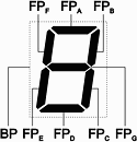
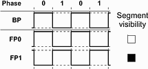
Static LCDs have only one background electrode and one terminal for each segment they can display. Therefore, 7-segment static display capable of displaying one digit will have eight terminals in total (Figure 3). Drive waveforms for such a display are shown in Figure 4. Voltage on the invisible segments approaches zero and voltage on the dark segments approaches full supply voltage. The drive bias therefore approaches infinity and no other drive scheme can be better as far as display contrast is concerned. This drive scheme is very simple to implement on general purpose I/Os of a microcontroller and this is why this type of display is very popular.
Drive of dynamic LCDs
If the driving scheme for static displays is so simple to implement why should we bother with any other type of LCDs? Since the static displays have one terminal for each segment, the number of terminals starts to rise very quickly when we try to add more digits on the same display. In case the LCD has pins (as opposed to rubber strip or thermically bonded flat cable), the added pins increase the cost of the display. Another problem is to place all the terminals at the top and bottom edges of the display and it may therefore prove difficult to make the display small enough. Another fact is that we need one GPIO pin for each display segment on the microcontroller side. The higher the pin count of the microcontroller, the larger the package and cost (number of pins and package size contributes to the microcontroller cost more than one would guess). All these reasons led to attempts to organise the display segments into a matrix (just like buttons in a keyboard).
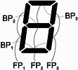
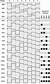
The dynamic LCDs (also called multiplexed) have multiple backplane electrodes and the frontplane pins are shared by multiple display segments. Example of dynamic LCD is shown in Figure 5. Now the challenge is to create waveforms for all the frontplane and backplane pins which would ensure that all the segments we want to appear invisible receive voltage below VT and all the segments we want to appear dark receive voltage above VS. How the waveforms should look like is far from obvious. Specialised LCD drive circuits and microcontroller peripherals normally use waveforms outlined in Figure 6 (shown for the case of four backplane electrodes). These waveforms have bias ratio of 1,73 and use four discrete voltage levels on all pins. It is easy to see that synthesis of these waveforms without the specialised circuit or peripheral would be quite difficult.
Fortunately, another driving scheme exists, which can be easily implemented on GPIO pins of a microcontroller. The modified waveforms are shown in Figure 7.
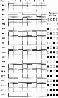
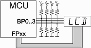
These have bias ratio of 1,53 (approx 12% lower than the original waveforms). The main advantage is that now we need just three discrete voltage levels for the backplane electrodes and only two voltage levels for the frontplane electrodes. This is much simpler to implement and a circuit similar to the one shown in Figure 8 can be used. The third (middle) voltage level on the backplane electrodes is achieved by configuring the GPIO pin in question as input and allowing the external resistors to define the voltage level. Of course, similar waveforms can be devised also for other numbers of backplane electrodes, waveforms for two backplane electrodes are shown in Figure 9.
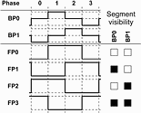
It is common property of all the driving schemes, that the bias ratio goes down with the number of backplane electrodes. Therefore, higher supply voltage of the microcontroller is needed for displays with higher level of multiplexing. Displays with two backplane electrodes can be driven from supply voltage of 3 V, however, displays with three and more backplane electrodes require higher supply voltages of the microcontroller. Since modern microcontrollers run happily from below 3 V up to 5 V, adjusting the supply voltage is the easiest way of matching the drive voltage requirements of a particular display. In case the supply voltage of the microcontroller is fixed at 5 V, dummy cycles can be introduced into the driving scheme to lower the voltages between the display electrodes.
Driving algorithm
An algorithm for driving the display can be devised from the driving waveforms. An example algorithm for display with four backplane electrodes is shown in Table 1.
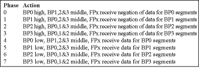
This algorithm is relatively easy to implement. Reaction times of TN displays depend on temperature and are usually around 150 ms. This allows relatively very slow refresh rates, display manufacturers usually recommend rates around 30 Hz. Since the above algorithm has eight phases, the required interrupt rate to drive the display is 240 Hz, which implies very low workload for the MCU. Using higher refresh rate only increases the microcontroller workload and power consumption (since the display is effectively a capacitive load).
For more information contact Daniel Malik, Motorola, [email protected], or Norman Ballard, Motorola SA, 021 946 3314, [email protected]

© Technews Publishing (Pty) Ltd | All Rights Reserved